L13 · Advanced Caches
Topic: memory · 61 pages
EECS 4340 Lecture 13 — Advanced Caches
Announcements

Show slide text
Announcements
- Project #4
- Due: 22-April-26
- Final exam
- Friday, May 8, 2026, 9 AM – 12 PM, Mudd 633
- Project meetings
- Mondays and Wednesdays during my office hours
Readings
Show slide text
Readings
For today:
- H & P Chapter 2.2, 2.3, and Appendix B.3
- Improving direct-mapped cache performance by the addition of a small fully-associative cache and prefetch buffers, https://dl.acm.org/doi/abs/10.1145/325096.325162
For next Monday:
- A primer on hardware prefetching, https://link.springer.com/book/10.1007/978-3-031-01743-8
Recap: Basic Caches
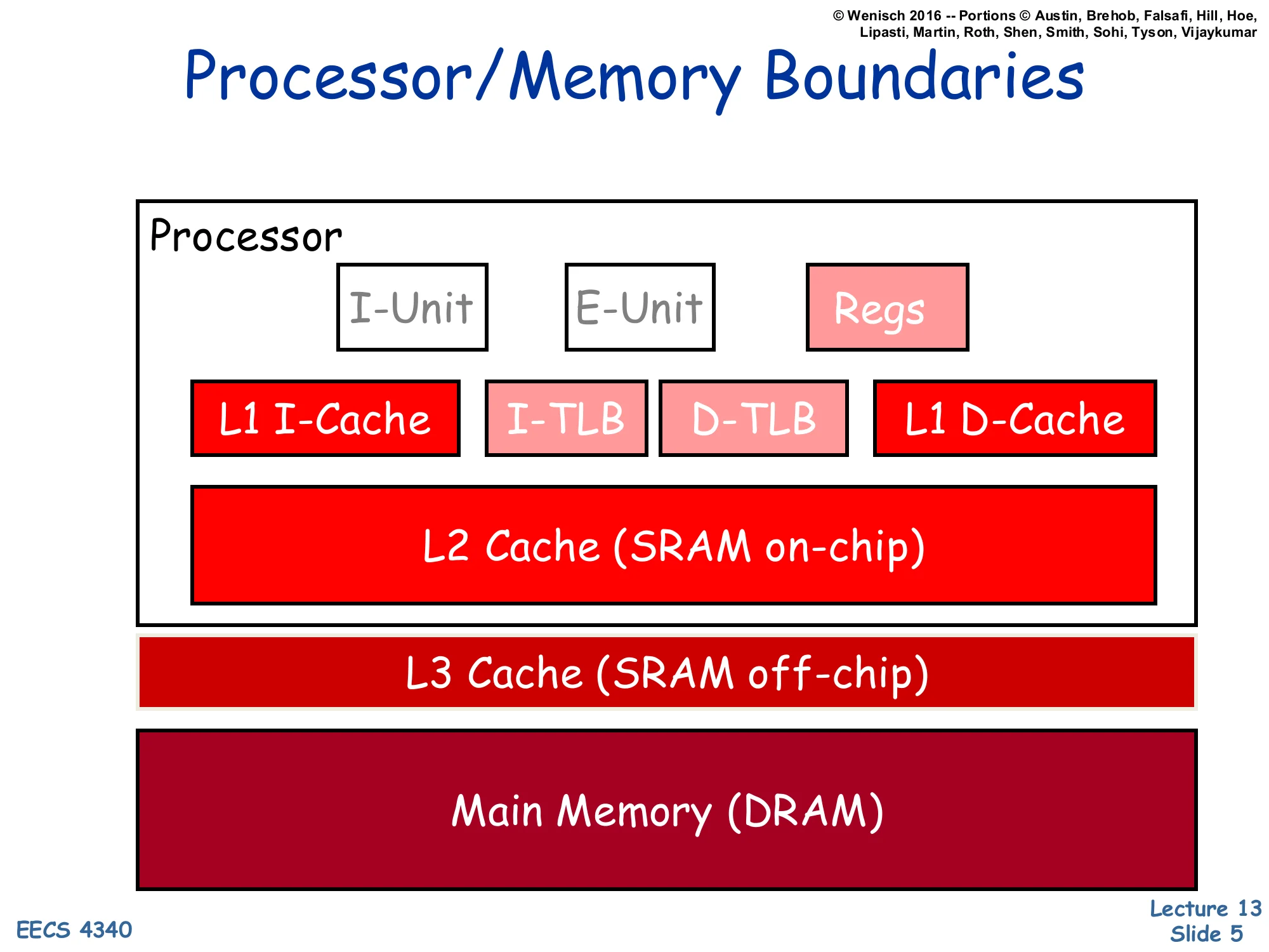
Processor/Memory Boundaries
Show slide text
Processor/Memory Boundaries
Processor (on-chip):
- I-Unit, E-Unit, Regs
- L1 I-Cache, I-TLB, D-TLB, L1 D-Cache
- L2 Cache (SRAM on-chip)
Off-chip:
- L3 Cache (SRAM off-chip)
- Main Memory (DRAM)
The picture shows the canonical multi-level memory hierarchy that this lecture optimizes. The processor core (instruction fetch / execute / register file) sits next to the fastest, smallest storage: split L1 instruction and data caches and the TLBs that translate addresses for them. A unified L2 SRAM lives on the same die but is 5–10× larger and slower than L1; an off-chip L3 (also SRAM) absorbs L2 misses before requests fall all the way through to DRAM. Each step down is roughly 10× larger and 10× slower, which is exactly the property that makes caches work — because of locality the average access time is dominated by hits at the top, while capacity is dominated by storage at the bottom. Almost every “advanced cache” trick later in the lecture (multi-level inclusion, NUCA, multi-banking, victim caches) makes sense only relative to this picture: where in the hierarchy a structure sits dictates its area, latency, bandwidth, and miss-cost budget.
Terminology
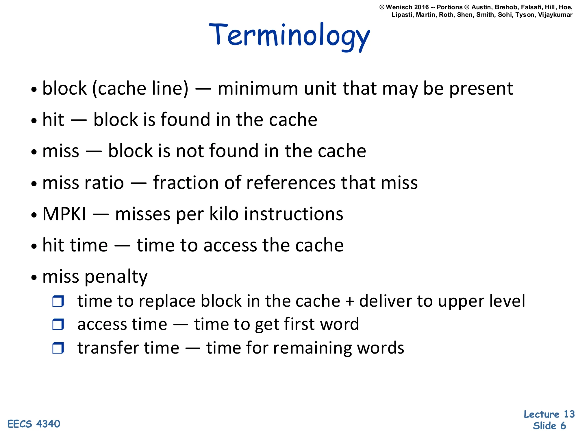
Show slide text
Terminology
- block (cache line) — minimum unit that may be present
- hit — block is found in the cache
- miss — block is not found in the cache
- miss ratio — fraction of references that miss
- MPKI — misses per kilo instructions
- hit time — time to access the cache
- miss penalty
- time to replace block in the cache + deliver to upper level
- access time — time to get first word
- transfer time — time for remaining words
These vocabulary items are the operational handles for every cache analysis in the lecture. A cache block (line) is the granularity of allocation, replacement, and transfer — you never bring in a single byte. Miss ratio is the natural per-reference probability, while MPKI normalizes by instruction count and is more useful for comparing programs of different memory intensities. Hit time is what shows up directly in the AMAT equation tavg=thit+miss-ratio×tmiss. Miss penalty itself decomposes into access time — getting the requested (“critical”) word — and transfer time — the rest of the line. That decomposition matters because optimizations like critical-word-first and early restart attack only the access-time component, while sub-blocking tries to limit how much transfer time you pay for a miss.
Fundamental Cache Parameters that affect miss rate
Show slide text
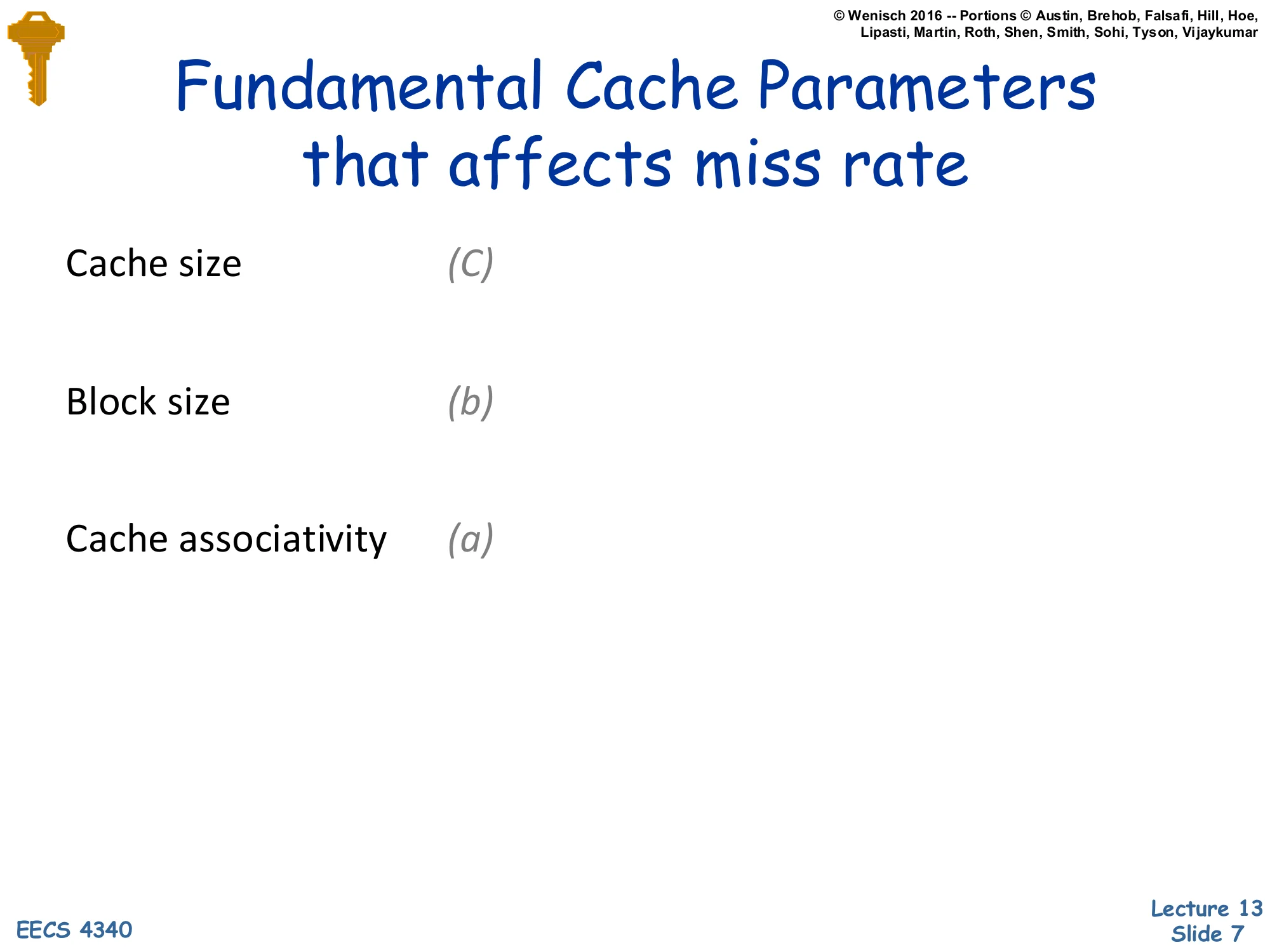
Fundamental Cache Parameters that affects miss rate
- Cache size (C)
- Block size (b)
- Cache associativity (a)
Three knobs determine the miss rate of a conventional cache: total capacity C, block size b, and associativity a. They interact: the number of sets is S=C/(a⋅b), so increasing associativity at fixed C,b reduces the number of sets (more ways per set, fewer sets); doubling block size at fixed C halves the number of blocks. Capacity primarily attacks capacity misses (working-set spillage), block size attacks compulsory misses via spatial locality (one miss now brings in neighbors), and associativity attacks conflict misses by giving each address more than one home. Each parameter has diminishing returns and a downside — bigger C is slower, bigger b wastes bandwidth and increases conflict, higher a raises hit-time and energy. The rest of L13 introduces tricks that improve one of these three terms without paying the usual cost (e.g., a victim cache improves effective associativity without growing the main array’s hit-time).
Associative Block Replacement
Show slide text
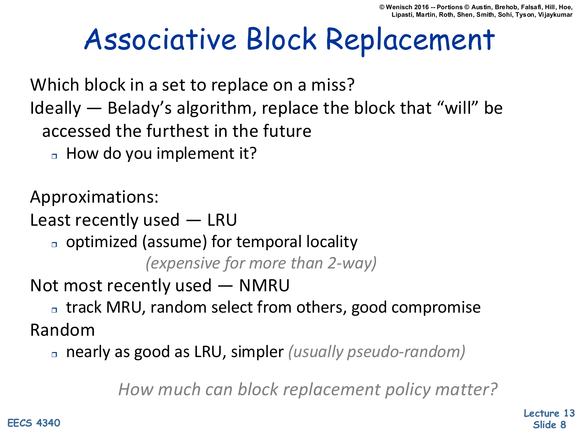
Associative Block Replacement
Which block in a set to replace on a miss?
Ideally — Belady’s algorithm, replace the block that “will” be accessed the furthest in the future
- How do you implement it?
Approximations:
- Least recently used — LRU
- optimized (assume) for temporal locality
- (expensive for more than 2-way)
- Not most recently used — NMRU
- track MRU, random select from others, good compromise
- Random
- nearly as good as LRU, simpler (usually pseudo-random)
How much can block replacement policy matter?
Once a set is full, the cache must pick a victim to evict. Belady’s MIN — replace the block whose next reference is the farthest in the future — is provably optimal but requires future knowledge, so it serves only as a comparison baseline. LRU approximates Belady by exploiting temporal locality, but exact LRU requires O(log2a!) bits of state per set and an a-way priority update on every hit, so it is impractical past 2-way. NMRU collapses the policy to a single bit (just remember which way was MRU and pick randomly among the rest); it is most of LRU’s benefit at a fraction of the cost. Pure random is even cheaper and within a few percent of LRU on most benchmarks. Modern processors typically use tree-PLRU or RRIP variants, all of which sit on this same spectrum: cost vs. how closely they approximate Belady. The lecture’s parenthetical question is a tease — replacement matters most when the working set is just barely larger than the cache.
Write Policies
Show slide text
Write Policies
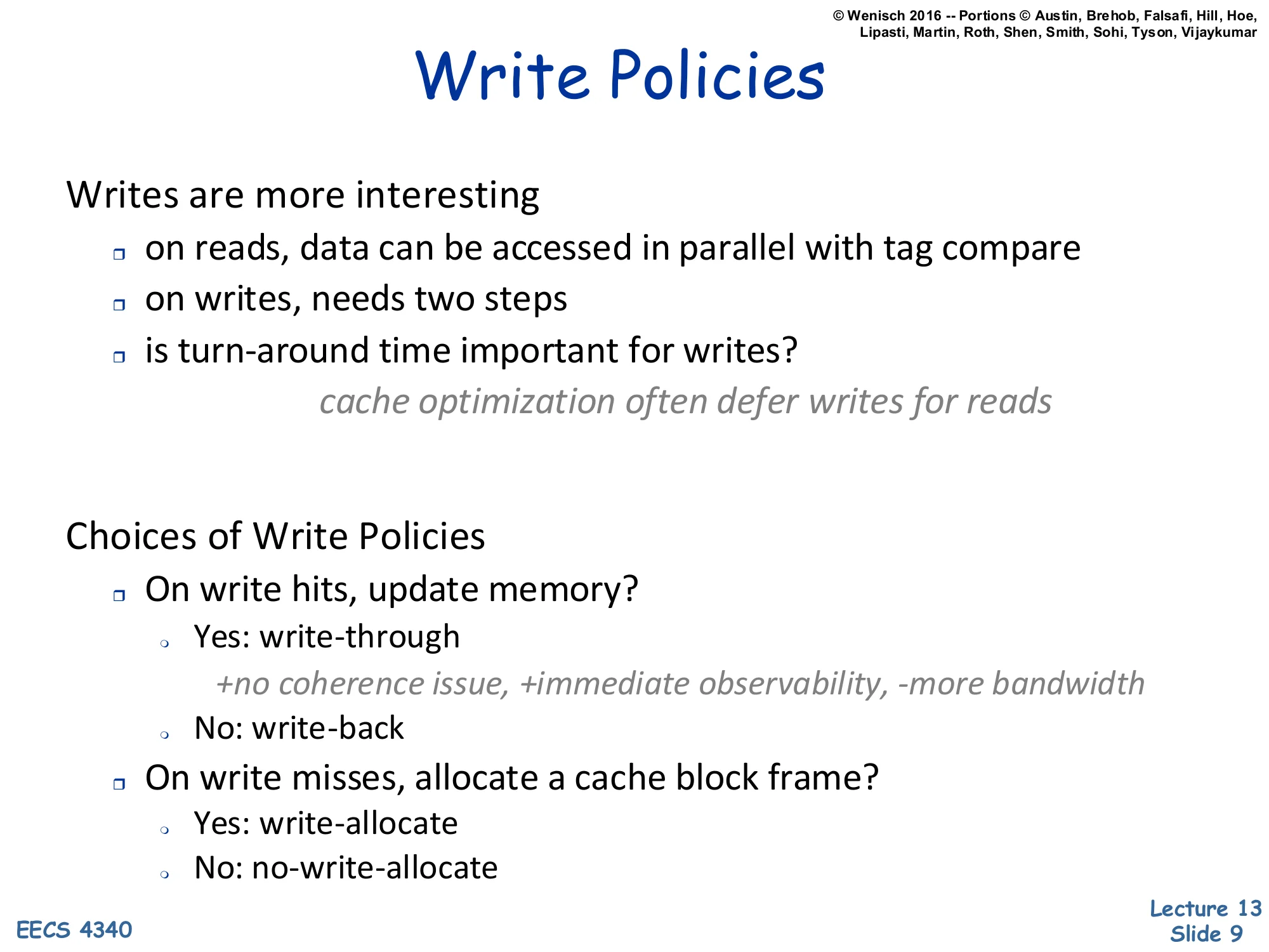
Writes are more interesting
- on reads, data can be accessed in parallel with tag compare
- on writes, needs two steps
- is turn-around time important for writes?
- cache optimization often defer writes for reads
Choices of Write Policies
- On write hits, update memory?
- Yes: write-through (+no coherence issue, +immediate observability, −more bandwidth)
- No: write-back
- On write misses, allocate a cache block frame?
- Yes: write-allocate
- No: no-write-allocate
Reads can speculatively read data and tag in parallel and discard the data on a tag mismatch — there is no harm because reads have no side effects. Writes are sequential by nature: the cache must verify the tag before mutating the cell, otherwise a miss could corrupt an unrelated line. Two orthogonal questions then define every write policy. On a hit, do you propagate to the next level immediately (write-through) or only on eviction (write-back using a dirty bit)? Write-through simplifies coherence (the next level is always current) but burns bus bandwidth on every store; write-back coalesces repeated stores to the same line into one writeback at eviction. On a miss, do you bring the block in (write-allocate, the natural pairing with write-back so subsequent stores hit) or just push the store onward (no-write-allocate, the natural pairing with write-through). The common pairings are write-back + write-allocate (L1/L2 caches) and write-through + no-write-allocate (some L1s for simplicity).
Store Buffers
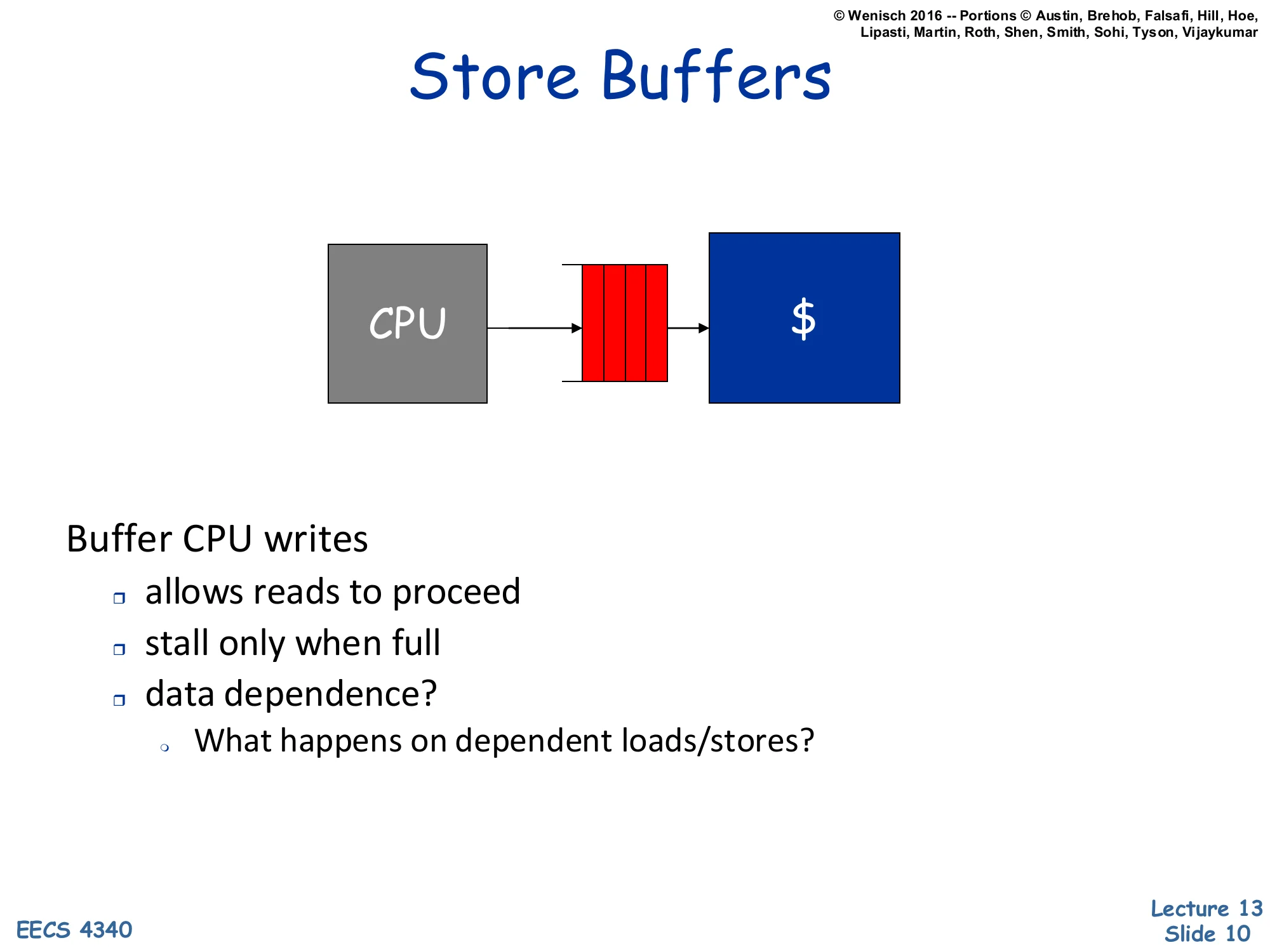
Show slide text
Store Buffers
[Diagram: CPU → store buffer (FIFO of pending writes) → $ (cache)]
Buffer CPU writes
- allows reads to proceed
- stall only when full
- data dependence?
- What happens on dependent loads/stores?
A store buffer decouples store retirement from cache update. Stores enqueue, the pipeline does not wait for the cache write to finish, and reads continue against the cache; stalls happen only when the buffer fills. This is essentially a small write-coalescing queue that hides write latency. The dependence question is the catch: if a younger load reads an address that an older store still sitting in the buffer wrote, the load must see the buffered value, not the stale cache value. In a real OoO core this is solved by store-to-load forwarding — the load CAM-matches its address against the buffer; on a hit it forwards the buffered data, on a partial overlap it stalls and replays. The L09 lecture on memory scheduling is where this gets a full treatment; here it is enough to understand that a store buffer is not just a passive FIFO — it participates in correctness.
Writeback Buffers
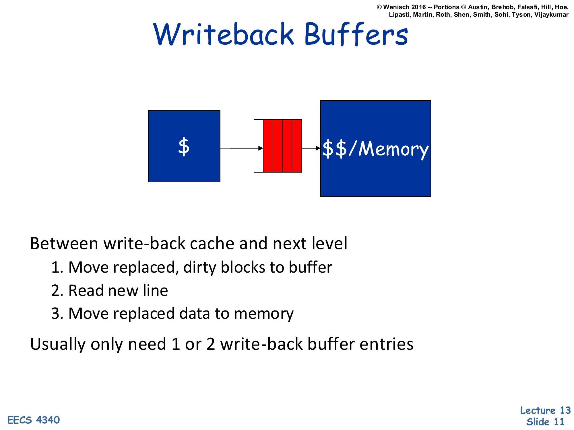
Show slide text
Writeback Buffers
[Diagram: $ → writeback buffer (FIFO) → $$ / Memory]
Between write-back cache and next level
- Move replaced, dirty blocks to buffer
- Read new line
- Move replaced data to memory
Usually only need 1 or 2 write-back buffer entries
A writeback buffer is the dual of the store buffer, sitting on the eviction path of a write-back cache. When a miss evicts a dirty line, the naive sequence “first write the dirty line back, then read the new line” doubles the miss latency. The writeback buffer breaks that ordering: the dirty line moves into the buffer, the new line is fetched from memory immediately into the freed frame, and the buffer drains the dirty line back to memory in the background. Because evictions are bursty (one per miss to a dirty set) but main memory consumes them at a steady rate, just one or two buffer entries usually suffice. A subtle requirement: subsequent fills/snoops must check the writeback buffer for the most recent copy, otherwise the system could read stale memory while the dirty line is still in flight.
Memory Systems: Advanced Caches
Memory Systems
Show slide text
Memory Systems
Basic caches
- introduction
- fundamental questions
- cache size, block size, associativity
Now:
- Advanced caches
- Main memory
- Virtual memory
This is a roadmap slide bridging L12 (basic caches) to the rest of the memory unit. “Basic caches” covered the three-parameter design space and the standard hit/miss machinery. “Advanced caches” — the rest of L13 — layers on miss-rate optimizations (skewed/way-predicting/victim caches), miss-penalty optimizations (critical word first, sub-blocking, multi-level), bandwidth optimizations (multi-banking, multi-porting, line buffers), and large-cache layout (NUCA). “Main memory” and “Virtual memory” come in subsequent lectures (L14 prefetching, L15 virtual memory). The grouping reflects the lecture’s analytic frame: every advanced technique targets one term of tavg=thit+miss-ratio×tmiss.
Advanced Caches
Show slide text
Advanced Caches
- Better miss rates
- Reducing miss penalty
- Higher bandwidth
- Beyond simple blocks
- Multi-level caches
- Prefetching
The six bullets are the lecture’s table of contents and they map directly onto the AMAT formula. “Better miss rates” reduces the miss-ratio term — covered by software restructuring, hash/skewed indexing, way-prediction, and victim caches. “Reducing miss penalty” reduces tmiss — covered by critical-word-first, early restart, and sub-blocking. “Higher bandwidth” lets a wide-issue core sustain multiple memory ops per cycle — multi-porting, multiple cache copies, multi-banking, line buffers. “Beyond simple blocks” is the sub-blocking topic. “Multi-level caches” introduces the L1/L2/L3 hierarchy with the inclusion property. “Prefetching” is its own lecture (L14). Every subsequent slide can be tagged with which AMAT term it improves.
Miss Classification (3+1 C's)
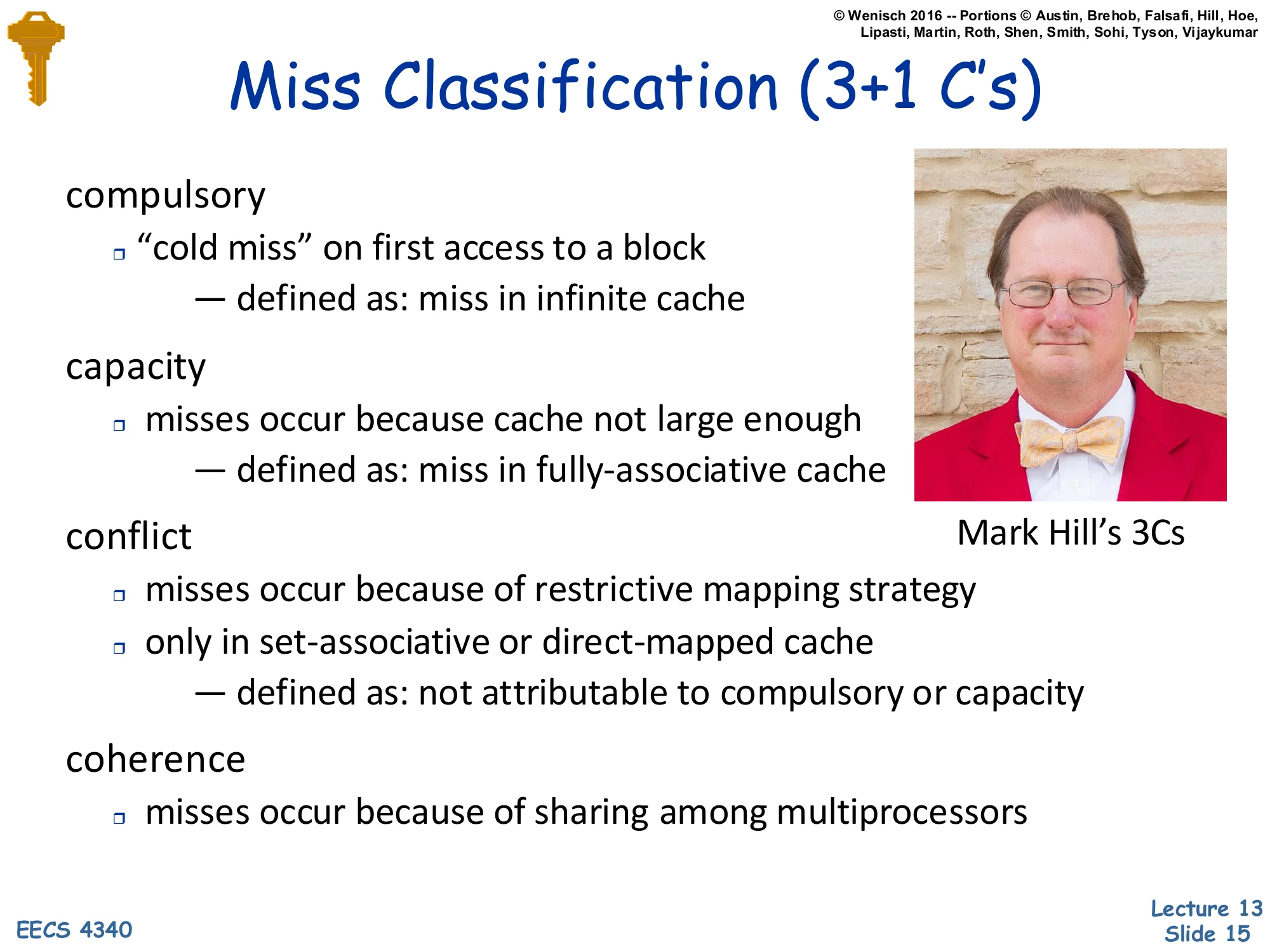
Show slide text
Miss Classification (3+1 C’s)
Mark Hill’s 3 Cs:
- compulsory
- “cold miss” on first access to a block
- defined as: miss in infinite cache
- capacity
- misses occur because cache not large enough
- defined as: miss in fully-associative cache
- conflict
- misses occur because of restrictive mapping strategy
- only in set-associative or direct-mapped cache
- defined as: not attributable to compulsory or capacity
- coherence
- misses occur because of sharing among multiprocessors
Mark Hill’s classification gives a definitional attribution scheme rather than a phenomenological one — each category is defined by the experiment that would eliminate it. Compulsory misses survive even an infinite cache because the line was never seen before. Capacity misses survive in a fully-associative cache of the right size but disappear when the cache is large enough to hold the working set. Conflict is the residual: misses that go away if you switch from a-way to fully-associative at the same capacity. The “+1” coherence miss appears only in multiprocessors when another core’s write invalidates a locally-cached line (covered in L16). The classification matters because each advanced technique targets a specific category — bigger blocks attack compulsory (spatial locality), bigger caches attack capacity, victim caches and skewed associativity attack conflict, and snoopy/directory protocols (L16) manage coherence.
How to Reduce Conflict Misses?
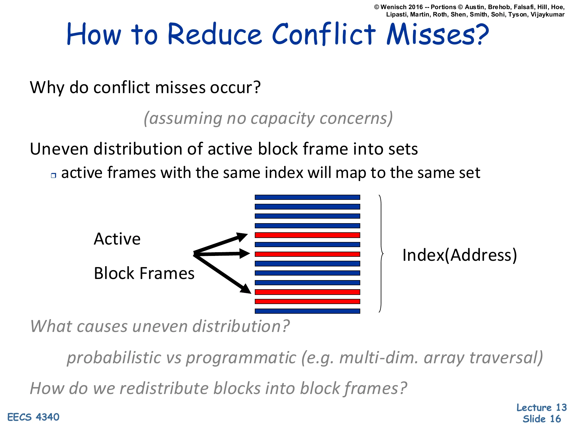
Show slide text
How to Reduce Conflict Misses?
Why do conflict misses occur? (assuming no capacity concerns)
Uneven distribution of active block frames into sets
- active frames with the same index will map to the same set
[Diagram: Active block frames concentrate in a few rows of Index(Address).]
What causes uneven distribution?
- probabilistic vs programmatic (e.g. multi-dim. array traversal)
How do we redistribute blocks into block frames?
The slide makes the conflict-miss problem visible: even when total capacity is plenty, the lines a program touches can pile up in a few sets simply because the address bits used for indexing happen to collide. The diagram shows red bands of “active” frames bunched together at certain index values. There are two regimes: probabilistic, where bad luck causes some sets to over-subscribe, and programmatic, where program structure deterministically forces collisions — the canonical example is striding through a 2-D array with a stride that is a power of two (so j+1 has the same index bits as j). Two solution families flow from this diagnosis: redistribute blocks (software approach — change the layout/access pattern) or redistribute into the set space differently (hardware approach — change the index function). The next several slides explore both.
Software Approach: Restructuring Loops and Array Layout
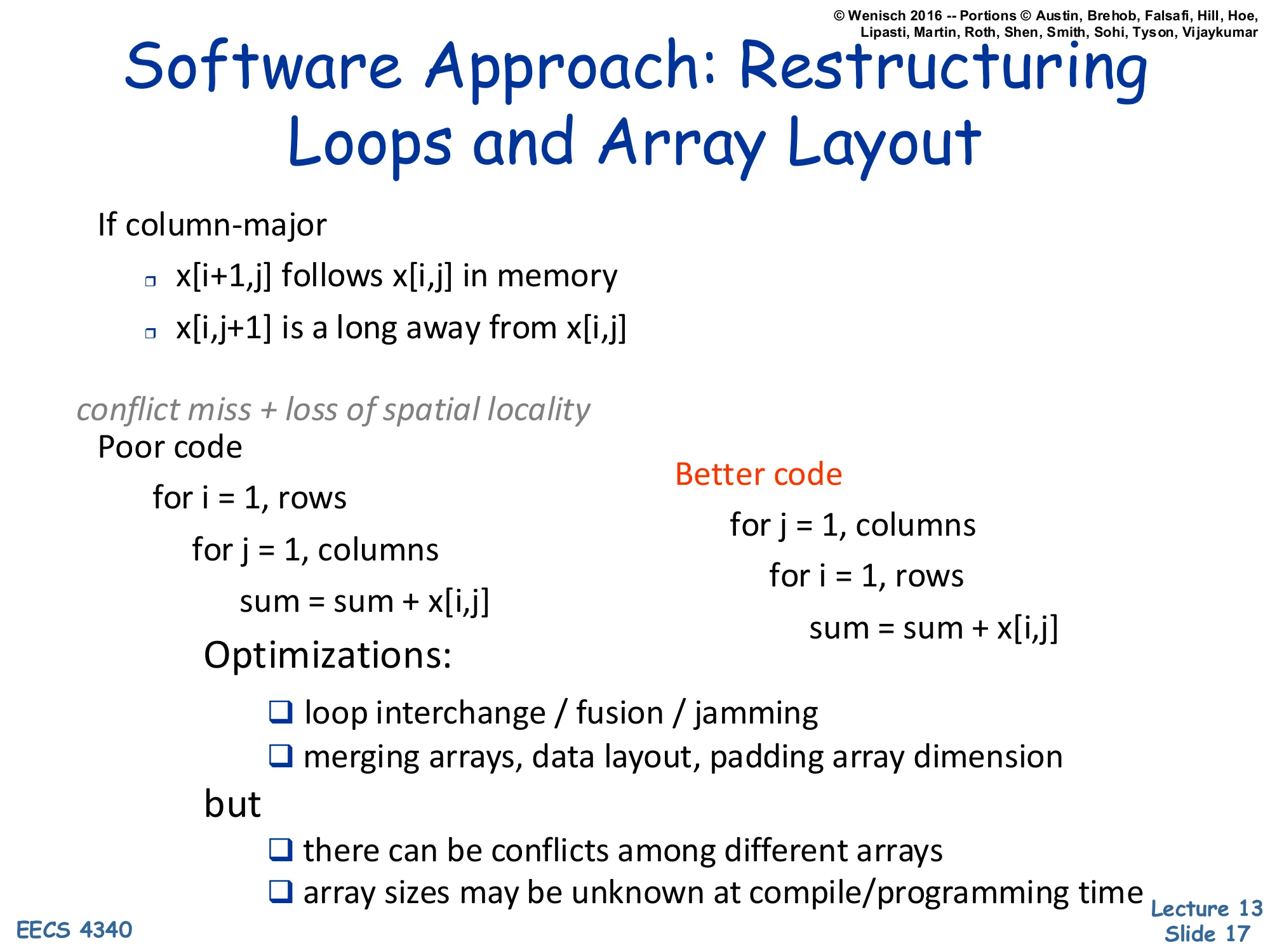
Show slide text
Software Approach: Restructuring Loops and Array Layout
If column-major:
- x[i+1,j] follows x[i,j] in memory
- x[i,j+1] is a long away from x[i,j]
conflict miss + loss of spatial locality
Poor code:
for i = 1, rows for j = 1, columns sum = sum + x[i,j]Better code:
for j = 1, columns for i = 1, rows sum = sum + x[i,j]Optimizations:
- ☐ loop interchange / fusion / jamming
- ☐ merging arrays, data layout, padding array dimension
but
- ☐ there can be conflicts among different arrays
- ☐ array sizes may be unknown at compile/programming time
Compilers and programmers can attack conflict and spatial-locality misses by changing the order of accesses or the layout of data. The example shows the canonical interchange: for a column-major language (Fortran), iterating by columns inside rows touches each row jumping a long stride into memory, causing both poor spatial locality (each access pulls in a line whose other words are unused) and probable conflict (consecutive rows of the same column have similar index bits). Reversing the loop nest matches the layout: consecutive iterations now hit consecutive words, every line is fully used. Other transformations include fusion (merging two loops over the same data), jamming (combining inner loops), array merging (interleaving fields so a struct-of-arrays becomes an array-of-structs), and dimension padding (adding an unused row to disrupt power-of-two strides). The two caveats explain why hardware help is also needed: cross-array conflicts and unknown sizes defeat purely-static layout choices.
Exposing Caches to Software
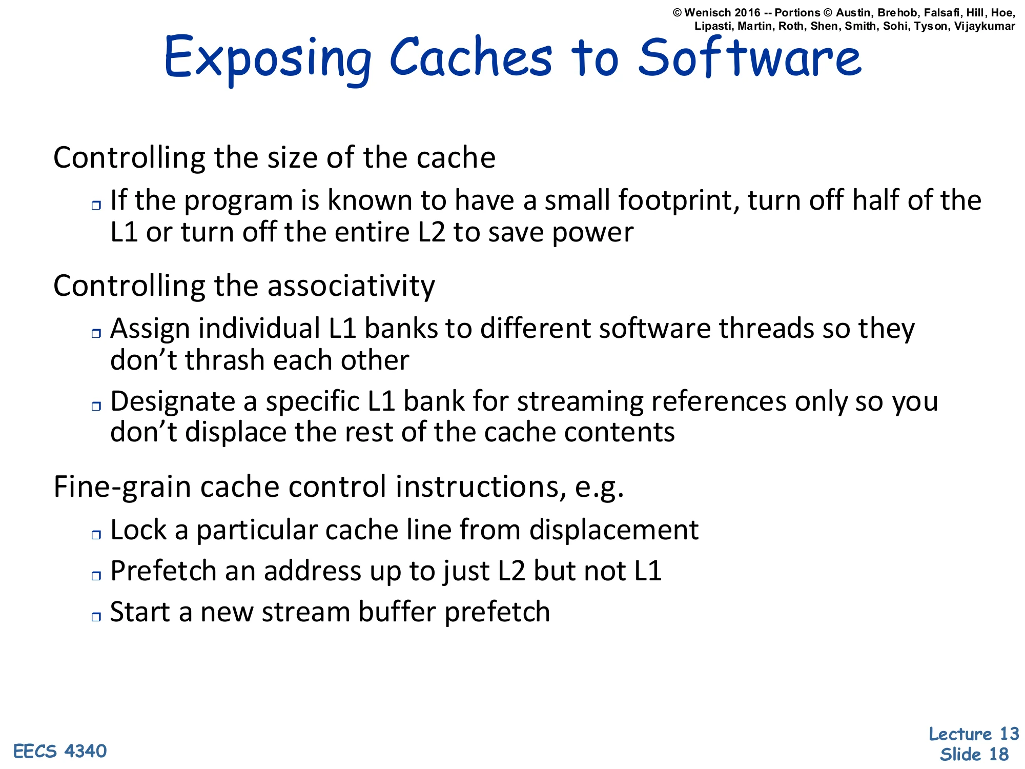
Show slide text
Exposing Caches to Software
Controlling the size of the cache
- If the program is known to have a small footprint, turn off half of the L1 or turn off the entire L2 to save power
Controlling the associativity
- Assign individual L1 banks to different software threads so they don’t thrash each other
- Designate a specific L1 bank for streaming references only so you don’t displace the rest of the cache contents
Fine-grain cache control instructions, e.g.
- Lock a particular cache line from displacement
- Prefetch an address up to just L2 but not L1
- Start a new stream buffer prefetch
Some advanced ISAs let software manage the cache directly instead of leaving everything to hardware policy. Capacity control — power down ways or whole levels when the working set is small — was added for power-constrained CPUs (the energy of an idle but powered SRAM is non-trivial). Associativity control — pinning specific ways to specific threads — turns the cache into a partitioned resource, useful in real-time and SMT settings to bound interference. Streaming-only ways isolate non-temporal references (like a video memcpy) so they do not pollute the cache with data that will not be reused. Fine-grain instructions let the program lock a hot cache line, prefetch into a specific level (e.g., to keep L1 free for demand traffic), or kick off a stream buffer. These extensions trade off the cache’s traditional transparency for predictability and power; almost every real ISA has at least cache-line lock and prefetch hint instructions.
Software-Assisted Cache Hierarchies
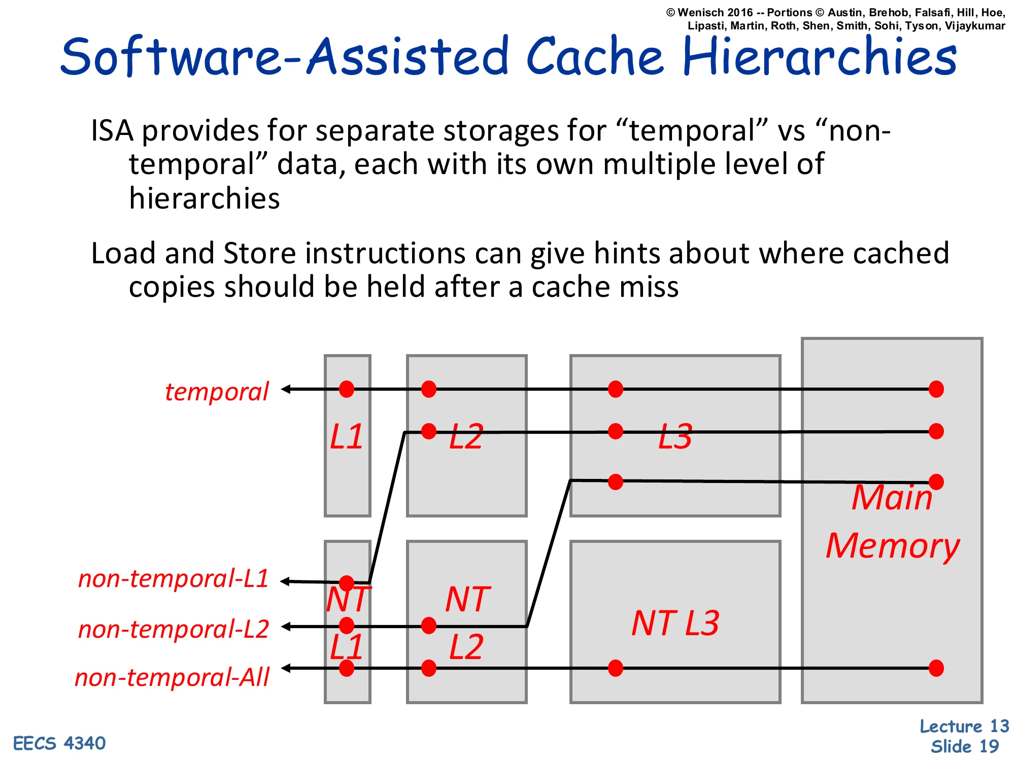
Show slide text
Software-Assisted Cache Hierarchies
ISA provides for separate storages for “temporal” vs “non-temporal” data, each with its own multiple level of hierarchies
Load and Store instructions can give hints about where cached copies should be held after a cache miss
[Diagram: parallel hierarchies — temporal path L1 → L2 → L3 → Main Memory, vs. non-temporal-L1 (NT only at L1), non-temporal-L2 (NT at L1+L2), non-temporal-All (NT path through everything to memory).]
A more aggressive form of ISA cache control splits the cache hierarchy in two: a temporal path (cache normally) and a non-temporal path (cache more conservatively or not at all). Loads/stores carry a hint that selects which path the line takes after a miss. The diagram enumerates the choices: a non-temporal load can be cached only in L1 (non-temporal-L1), only in L2 (non-temporal-L2), or bypass all caches (non-temporal-All) — each successive choice promises less reuse and avoids polluting more levels. Real ISAs include this idea in instructions like x86’s MOVNT* (non-temporal stores that bypass the cache) and ARM’s load/store with hint. The benefit is sparing capacity for genuinely-reusable data; the cost is software now has to predict reuse. This slide is dense and the parallel-hierarchy diagram is hard to read at original resolution — the four arrow paths annotate which level each NT mode lands in.
Blocking Algorithm
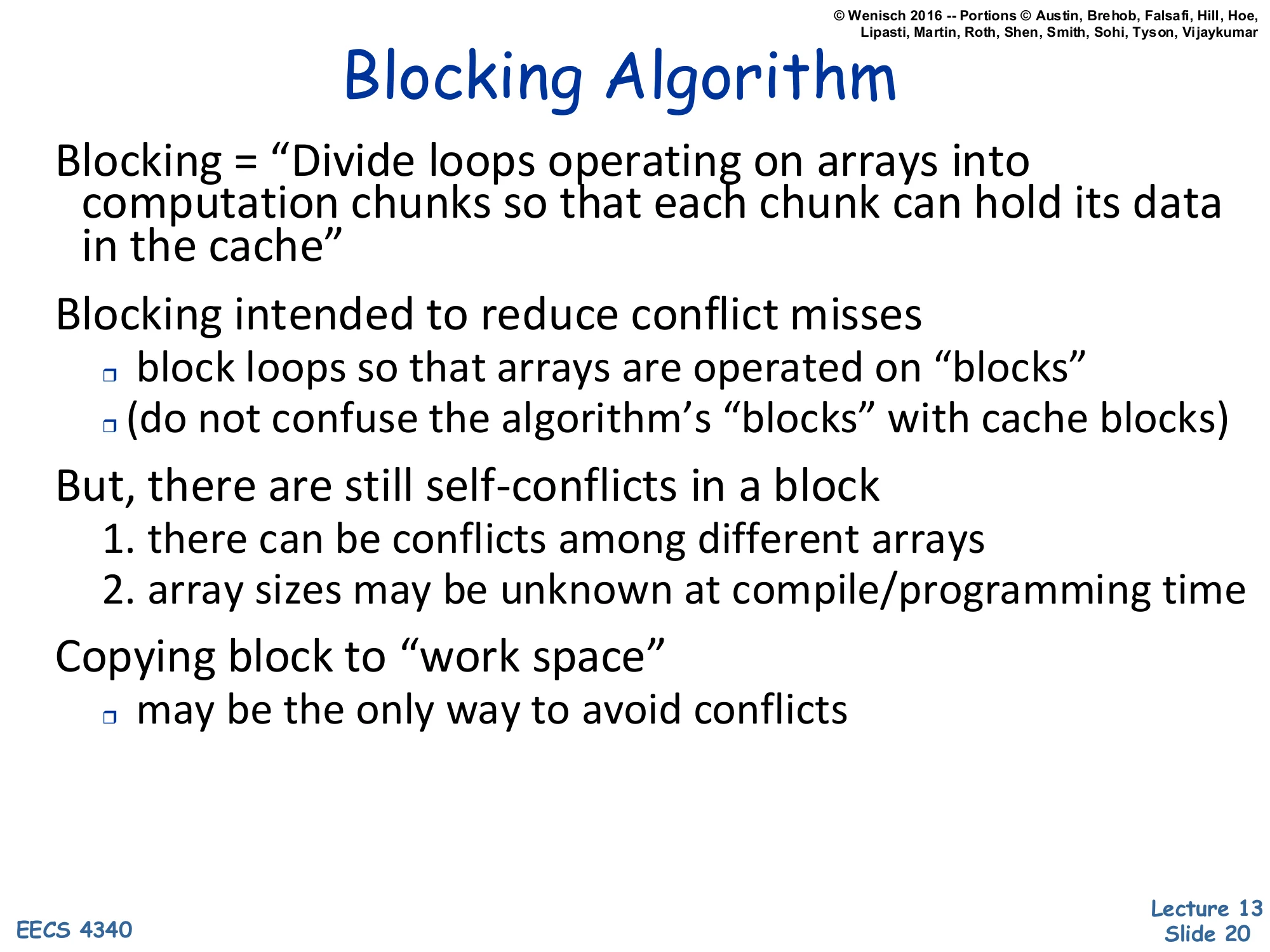
Show slide text
Blocking Algorithm
Blocking = “Divide loops operating on arrays into computation chunks so that each chunk can hold its data in the cache”
Blocking intended to reduce conflict misses
- block loops so that arrays are operated on “blocks”
- (do not confuse the algorithm’s “blocks” with cache blocks)
But, there are still self-conflicts in a block
- there can be conflicts among different arrays
- array sizes may be unknown at compile/programming time
Copying block to “work space”
- may be the only way to avoid conflicts
Blocking (also called tiling) is the classic algorithmic technique to fit a working set in the cache. The canonical example is matrix multiplication: instead of computing C=AB row-by-column over the whole matrix, partition A, B, C into b×b tiles and multiply tile-by-tile. Each tile pair fits in the cache, gets reused b times, and only then is the next pair brought in — a b-fold reduction in main-memory traffic. The slide’s two caveats are honest about why blocking is not a silver bullet. Self-conflicts happen when several tiles map to the same cache sets (conflict miss within a single tile because of bad address arithmetic). Cross-array conflicts happen when matrices A and B alias in the cache. Unknown sizes break compile-time tile-size selection. The escape hatch is to copy each tile into a contiguous scratch buffer once at tile-load time, paying a one-time linear cost to guarantee in-cache layout — used by many BLAS implementations. The slide is dense and somewhat low-resolution; legibility is acceptable but the bullet structure is the load-bearing content.
Hardware Approach: Use Hash Functions
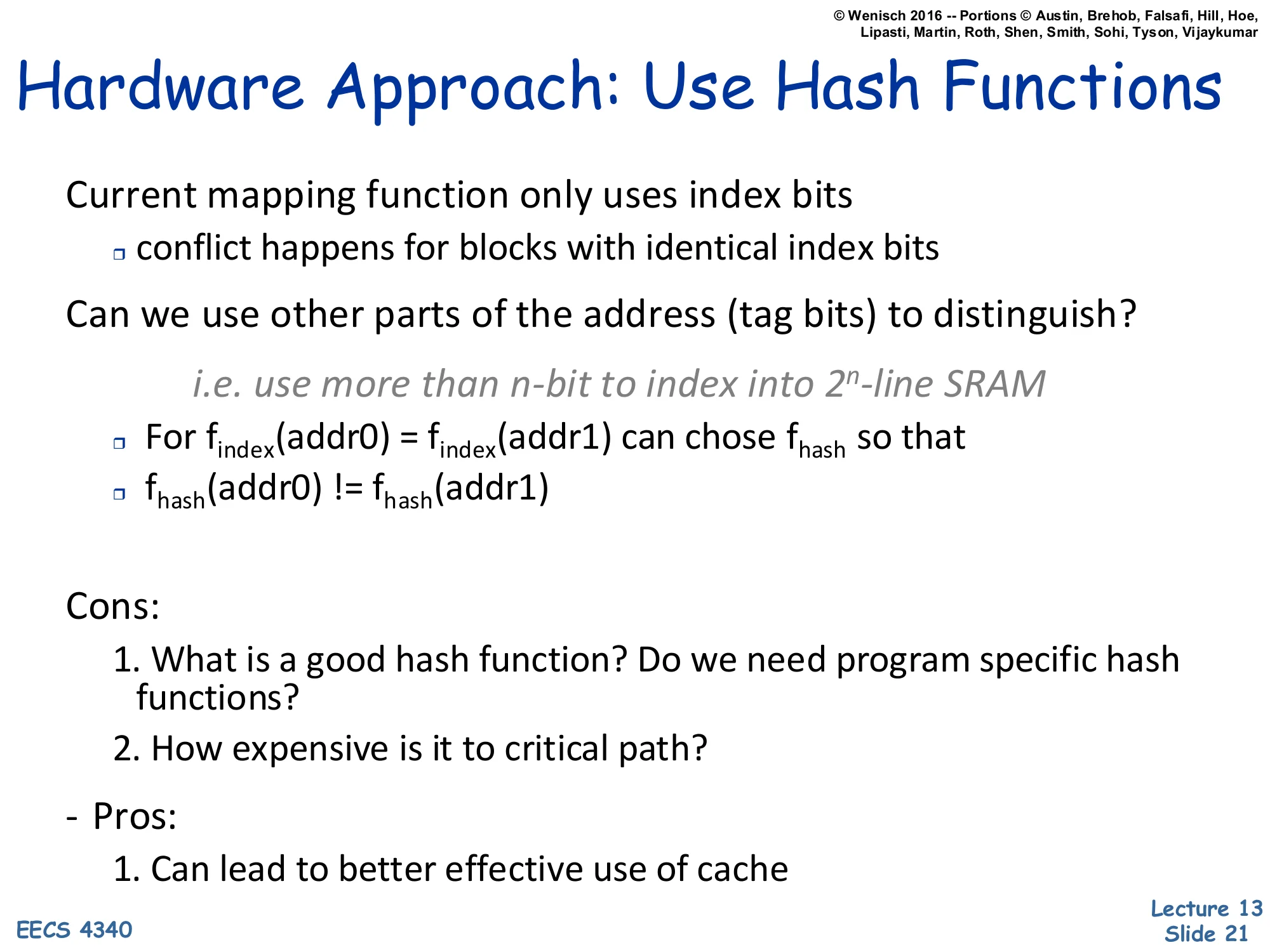
Show slide text
Hardware Approach: Use Hash Functions
Current mapping function only uses index bits
- conflict happens for blocks with identical index bits
Can we use other parts of the address (tag bits) to distinguish?
i.e. use more than n-bit to index into 2n-line SRAM
- For findex(addr0)=findex(addr1) can choose fhash so that
- fhash(addr0)=fhash(addr1)
Cons:
- What is a good hash function? Do we need program specific hash functions?
- How expensive is it to critical path?
Pros:
- Can lead to better effective use of cache
The standard cache index function takes a contiguous slice of address bits — the lower-middle bits between block-offset and tag. Two addresses that happen to share those bits collide regardless of how different the rest of the address is. The hardware fix is to compute the index with a hash function that mixes in tag bits too: even when two addresses have identical low index bits, their hashed indices differ if their upper bits differ. The simplest realization is a XOR-fold: idx′=idx⊕tag. This breaks programmatic stride conflicts — power-of-two strides through arrays now scatter across many sets. The trade-offs are real: choosing a hash that helps the average workload without hurting the worst case is hard (there is no universally optimal hash), and the XOR sits on the timing-critical decoder path so it must be very simple. Skewed-associative caches and column-associative caches (next slides) make this idea concrete.
Regular Set-Associative Cache
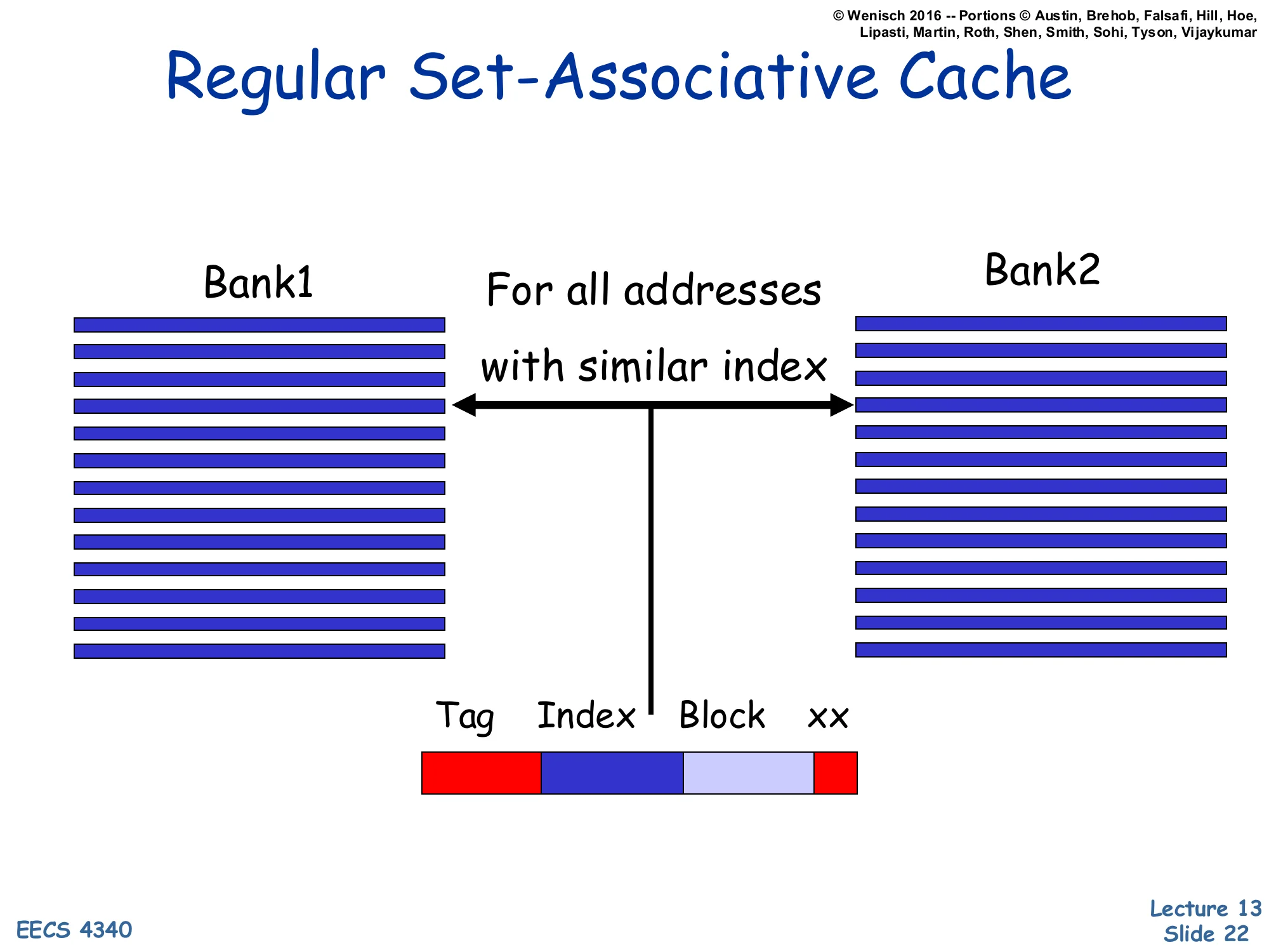
Show slide text
Regular Set-Associative Cache
[Diagram: Address divided into Tag | Index | Block | xx. Index drives both Bank1 and Bank2 (a 2-way set-associative cache). Both banks read the same row index — “For all addresses with similar index”.]
This is the baseline picture for the next slide’s contrast. In a standard 2-way set-associative cache, every address with the same index bits hits the same row in both banks — both ways are searched in parallel. The address decomposes into tag, index, block-offset, byte-offset. The set is uniquely determined by the index, and any two blocks whose addresses differ only in the tag fight over the same two slots. With the program-pathological stride pattern from earlier, several active addresses share the same index and the two-way capacity of that set is overwhelmed: conflict misses ensue even though plenty of other sets are empty. The skewed-associative design on the next slide breaks this lockstep by letting each bank use a different index function, so the set of active blocks gets spread across multiple rows in different banks instead of piling up in one row.
Seznec's Skewed-Associative Cache
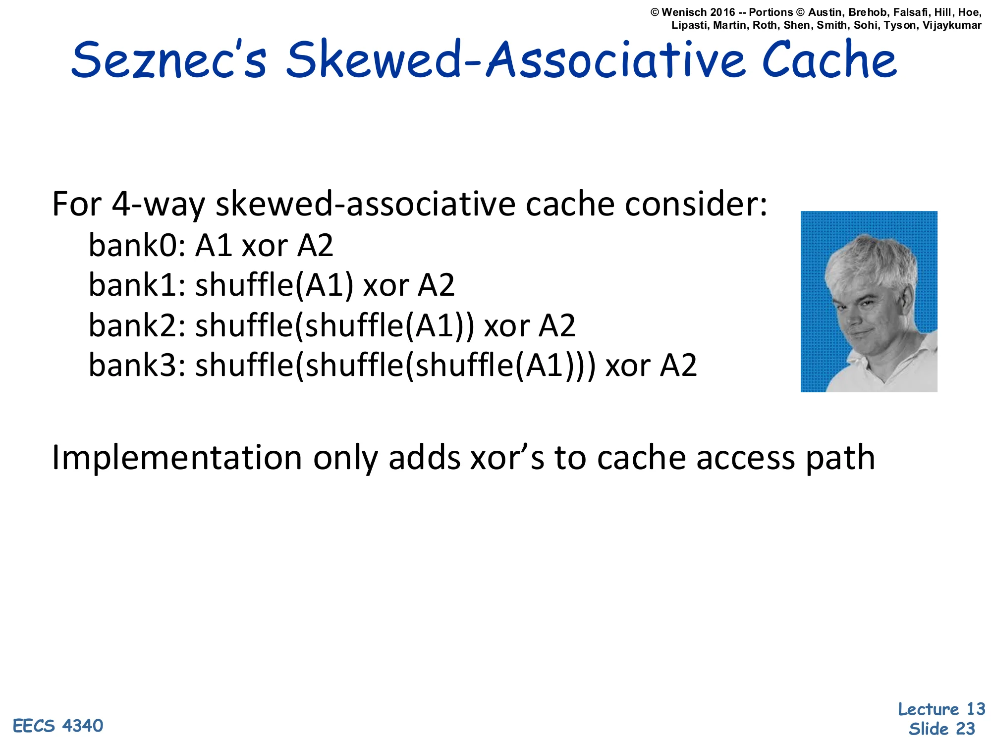
Show slide text
Seznec’s Skewed-Associative Cache
For 4-way skewed-associative cache consider:
- bank0: A1 xor A2
- bank1: shuffle(A1) xor A2
- bank2: shuffle(shuffle(A1)) xor A2
- bank3: shuffle(shuffle(shuffle(A1))) xor A2
Implementation only adds xor’s to cache access path
André Seznec’s skewed-associative cache gives each of the a banks a different index function. The slide’s example uses A1 and A2 as two slices of the address; bank 0 indexes by A1⊕A2, bank 1 by shuffle(A1)⊕A2, and so on, where each shuffle is a fixed bit-permutation. The crucial property: for any two addresses, even if they collide in one bank’s index, they almost certainly do not collide in the other banks. Conflict misses thus require collisions in every bank simultaneously, which is exponentially less likely than collisions in a single bank. The hardware cost is small — a few XOR gates and bit-shuffle wires per bank decoder — but two complications arise: replacement is harder (no single “set” — each address belongs to a different set in each bank), and the access path is on the critical timing edge. Seznec’s result was that 2-way skewed often beats 4-way conventional in miss rate at lower hardware cost. The slide is dense; tag the entry as a proposed concept.
Seznec's Skewed-Associative Cache (diagram)
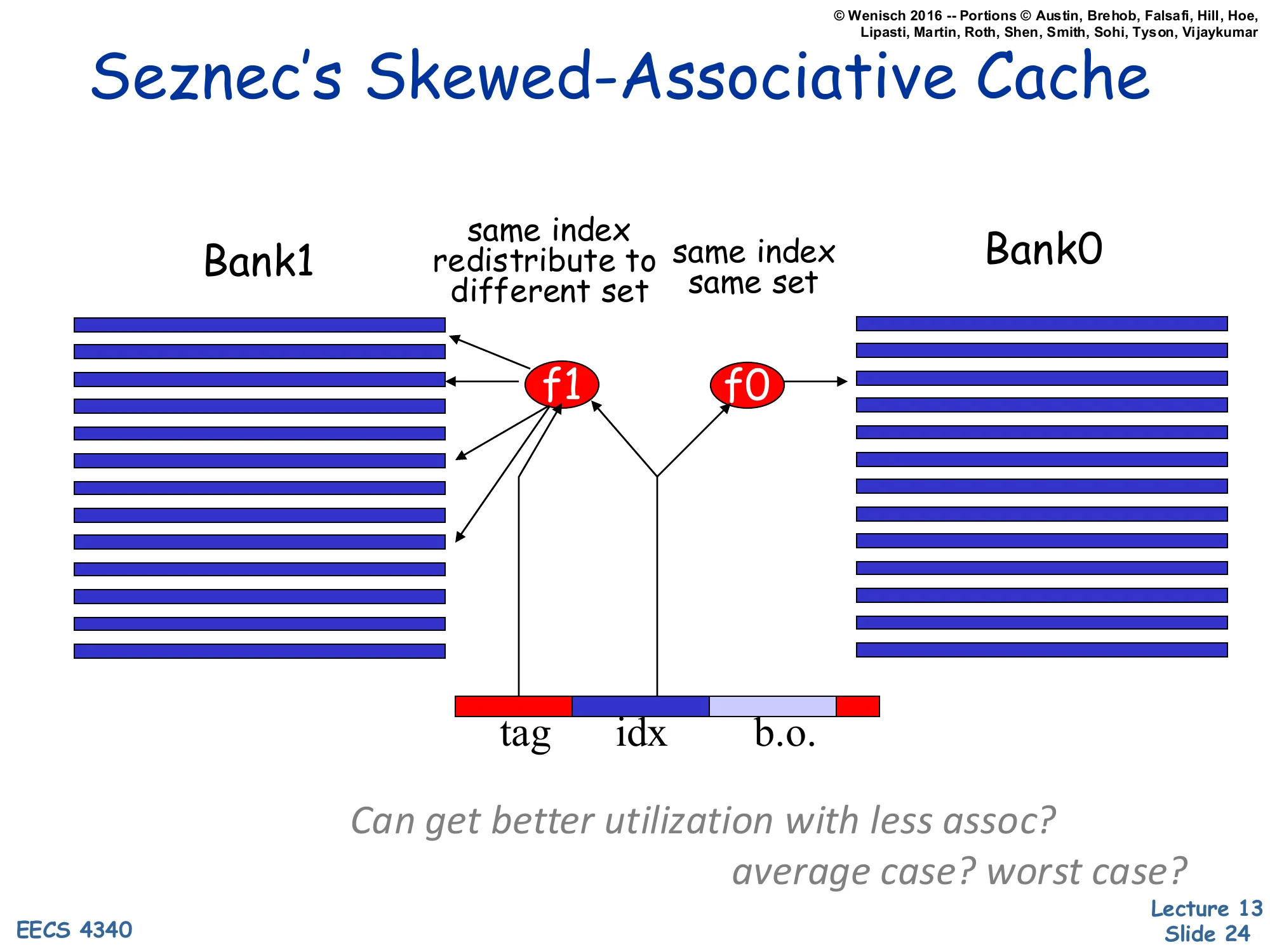
Show slide text
Seznec’s Skewed-Associative Cache
[Diagram: Address split into tag | idx | b.o. drives two index hashers f0 and f1. f0 maps to Bank0 (“same index, same set”). f1 maps to Bank1 with a different shuffle, so two addresses with identical idx can land in different rows of Bank1 — “same index redistribute to different set”.]
Can get better utilization with less assoc? average case? worst case?
The diagram makes the redistribution visible. A single address’s idx bits drive two hash functions f0 (just identity into Bank0) and f1 (a XOR/shuffle into Bank1). Two addresses that share idx bits — and so would share a set in a normal 2-way cache — share the same set in Bank0 but land in different rows of Bank1. The probability that they collide in both banks is much smaller than the probability they collide in one. The italic question challenges the design: can a 2-way skewed cache match a 4-way conventional cache? On average, yes — published results show skewing buys roughly one extra way of effective associativity. The worst case is harder to bound: an adversarial address sequence could still pile up in a single bank’s hash. The diagram is reasonably legible; the arrows and bank labels are the load-bearing visual content.
Column-Associative Cache
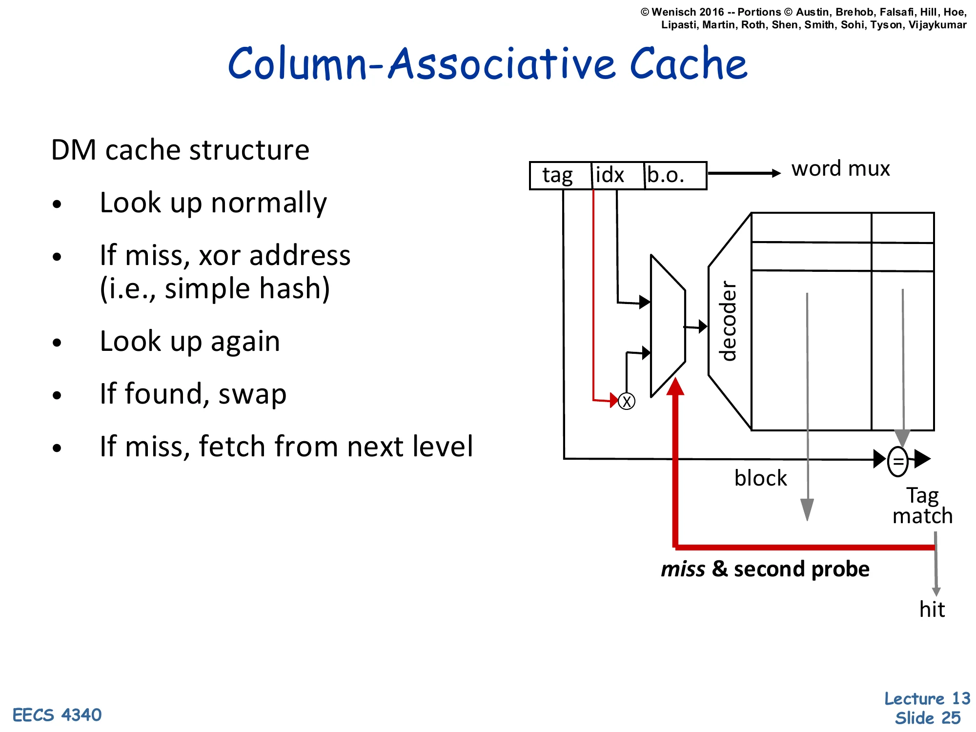
Show slide text
Column-Associative Cache
DM cache structure
- Look up normally
- If miss, xor address (i.e., simple hash)
- Look up again
- If found, swap
- If miss, fetch from next level
[Diagram: A direct-mapped cache where on a miss, the index is XOR’d with a tag bit and re-probed. A second tag-match on the second probe = hit; if it matches, the two lines swap so the freshly-accessed line lives in the primary slot.]
A column-associative cache is a clever way to get 2-way effective associativity from a single direct-mapped array. The first probe is a normal direct-mapped lookup. On a miss, the cache flips a single bit of the index (a trivial hash) and probes a second time. A hit on the second probe is reported as a regular hit (with one extra cycle of latency) and the two lines are swapped so that the freshly-accessed line moves to the primary slot — making future accesses to it fast again. This effectively gives each address two homes (its primary index and its hashed alternate) but uses only direct-mapped hardware. The pros are area near direct-mapped and miss rate near 2-way; the cons are variable hit latency and the swap traffic. The diagram is dense; the red arrow shows the second probe path on the cache structure.
Pseudo-Associativity: e.g. MIPS R10K 2-way L2
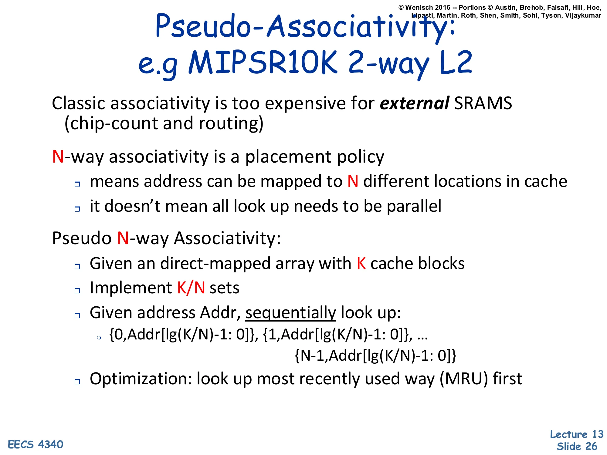
Show slide text
Pseudo-Associativity: e.g. MIPS R10K 2-way L2
Classic associativity is too expensive for external SRAMs (chip-count and routing)
N-way associativity is a placement policy
- means address can be mapped to N different locations in cache
- it doesn’t mean all look ups need to be parallel
Pseudo N-way Associativity:
- Given an direct-mapped array with K cache blocks
- Implement K/N sets
- Given address Addr, sequentially look up:
- {0, Addr[lg(K/N)−1: 0]}, {1, Addr[lg(K/N)−1: 0]}, … {N−1, Addr[lg(K/N)−1: 0]}
- Optimization: look up most recently used way (MRU) first
Pseudo-associativity decouples the associativity policy (each address has N possible homes) from the access implementation (parallel vs sequential probing). On an external SRAM where parallel access requires N separate chips with separate routing, this decoupling is essential — you cannot afford the pin count. The MIPS R10000 used 2-way pseudo-associative external L2: a direct-mapped array with K blocks is logically partitioned into K/N sets, and on a miss the cache re-probes with a different way bit prepended to the index. The MRU-first optimization keeps average hit latency close to single-probe (because most hits are in the recently-used way), while cold or thrashing accesses pay the second probe. The technique is similar in spirit to column-associative — both use sequential probes — but column-associative typically targets L1 with bit-flip hashing, whereas pseudo-associative targets L2/L3 with way-bit prefixing. The slide is dense and somewhat low-resolution; legibility is acceptable.
Way-Predicting Set-Associative Cache
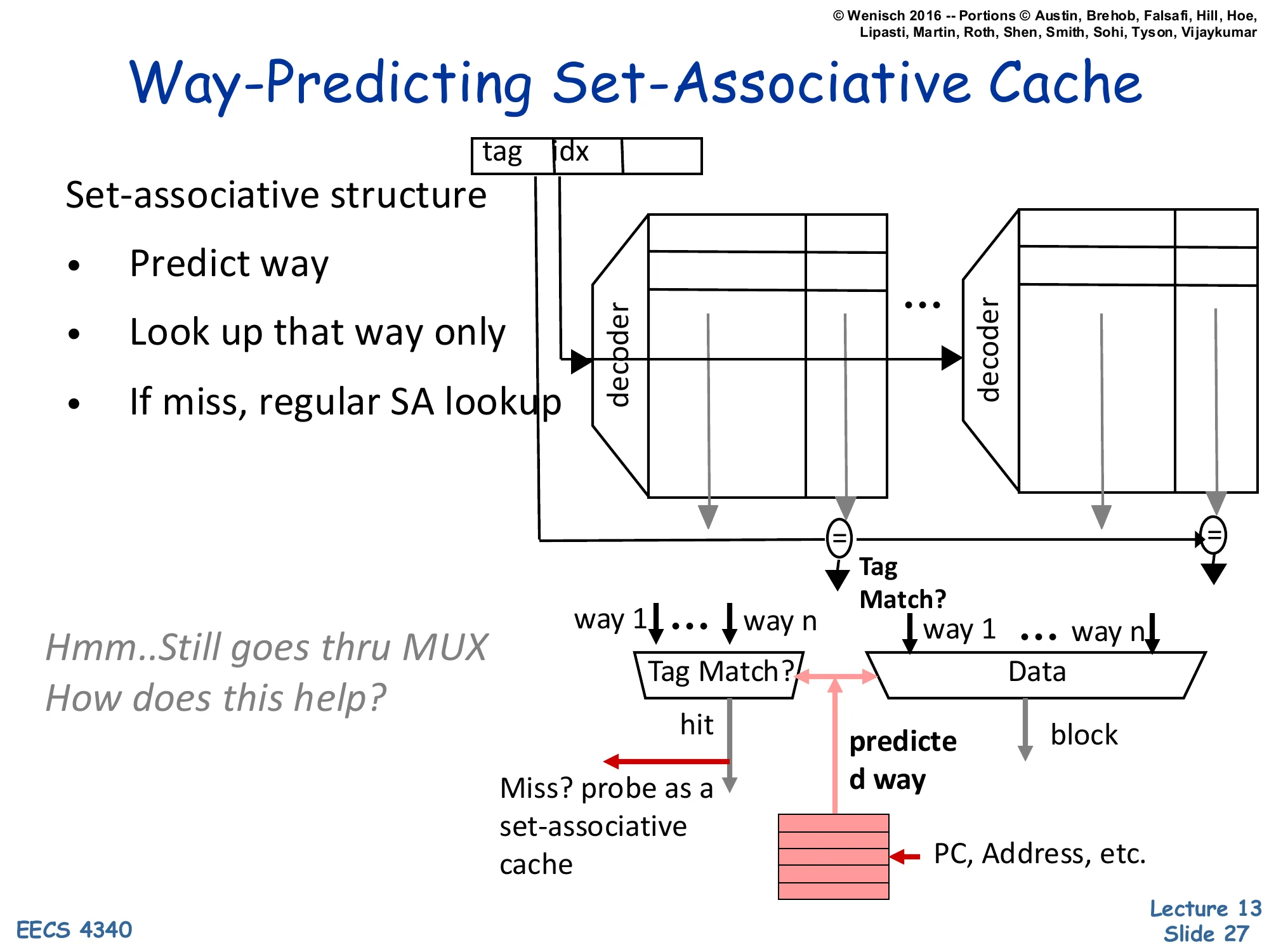
Show slide text
Way-Predicting Set-Associative Cache
[Diagram: Address (tag, idx) → set-associative banks with decoders per way. A way-predictor table indexed by PC/Address selects the predicted way. Only that way is read (saving energy); tag match validates. On miss, full SA lookup completes the search.]
Set-associative structure:
- Predict way
- Look up that way only
- If miss, regular SA lookup
Hmm… Still goes thru MUX. How does this help?
Way-prediction cuts the energy and (sometimes) the latency of set-associative access. A small predictor — indexed by PC, by the access address, or by both — guesses which of the N ways will hit; only that way’s data array is read. On a correct prediction, the cache delivers data after a single SRAM access plus tag check (vs N parallel data reads in conventional SA). On a misprediction, all ways are checked as a fallback, paying one extra cycle. The energy savings are dramatic because data SRAM reads dominate cache power, and only one is performed per access. The latency savings depend on whether the access path was previously gated by the way-MUX. The slide’s tease — “still goes through MUX” — points out that on a 2-way SA, the data MUX is small and not on the critical path, so way-prediction’s benefit is mostly energy. On 4-way or 8-way caches the data MUX is significant, and the latency savings become real. Used in Alpha 21264 L1, ARM Cortex variants, and many low-power designs.
Norm Jouppi's Victim Cache
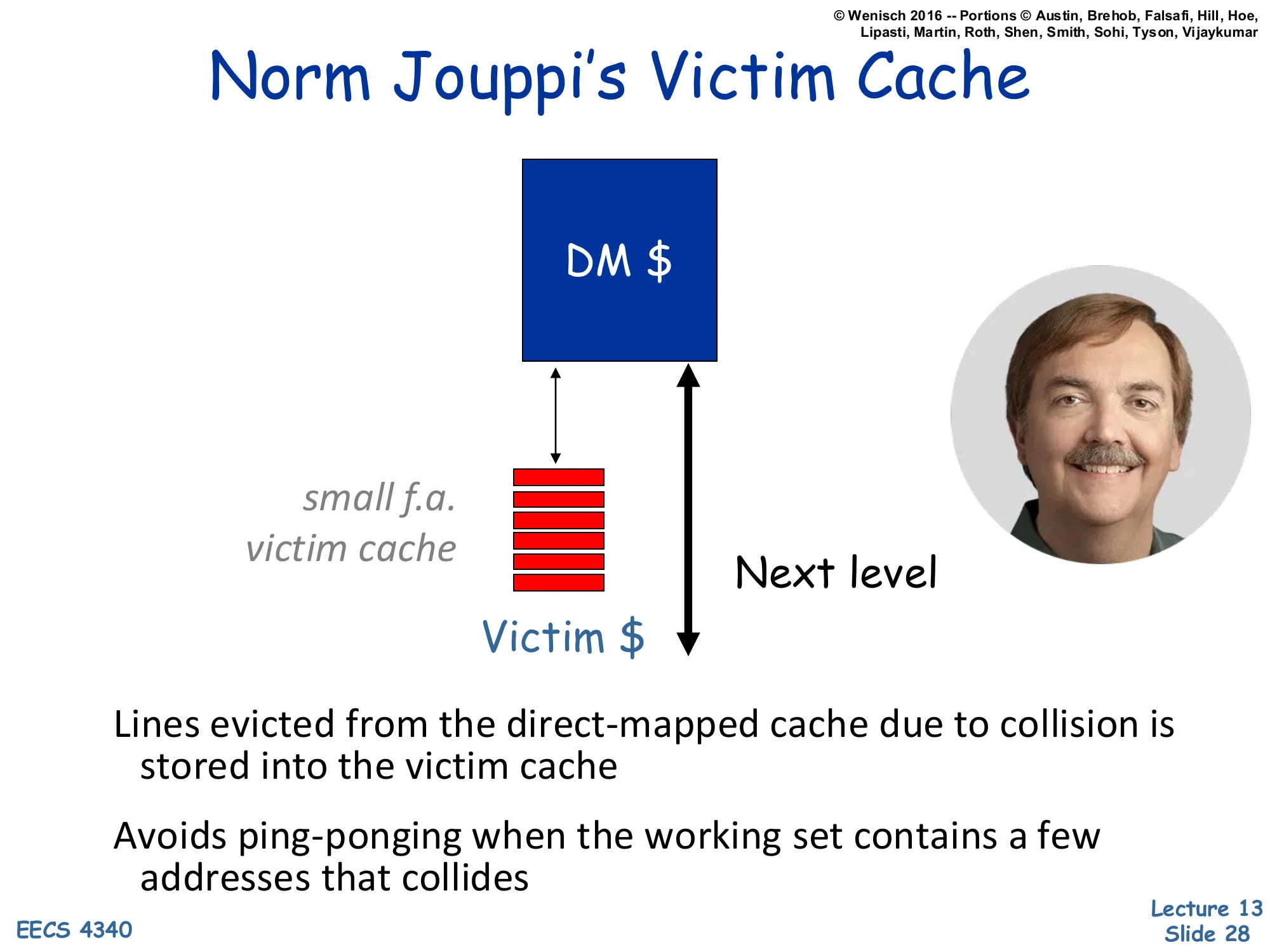
Show slide text
Norm Jouppi’s Victim Cache
[Diagram: A small fully-associative “Victim "sitsnexttotheDirect−Mappedmain"DM” cache. Evictions from DM go into Victim; on a DM miss, Victim is also probed; both the main cache and victim cache share the same path to the next level.]
Lines evicted from the direct-mapped cache due to collision is stored into the victim cache
Avoids ping-ponging when the working set contains a few addresses that collides
The victim cache is one of the most influential cache ideas — Jouppi 1990. A small fully-associative buffer (typically 4–16 entries) sits beside the direct-mapped main cache, not in series. When a line is evicted from the main cache because of a conflict, it goes into the victim cache instead of straight to the next level. On a subsequent main-cache miss, the victim is probed in parallel with the next-level request; if the line is in the victim, it is restored to the main cache (and the main-cache victim moves to the victim cache). The classic case it solves is a small working set with two or three addresses that map to the same direct-mapped set and ping-pong, evicting each other on every reference: with a victim cache, the displaced line is rescued from the victim and the ping-pong becomes a victim-cache hit cycle instead of a memory access. The next slide quantifies why even a tiny victim cache helps.
Norm Jouppi's Victim Cache (mechanism)
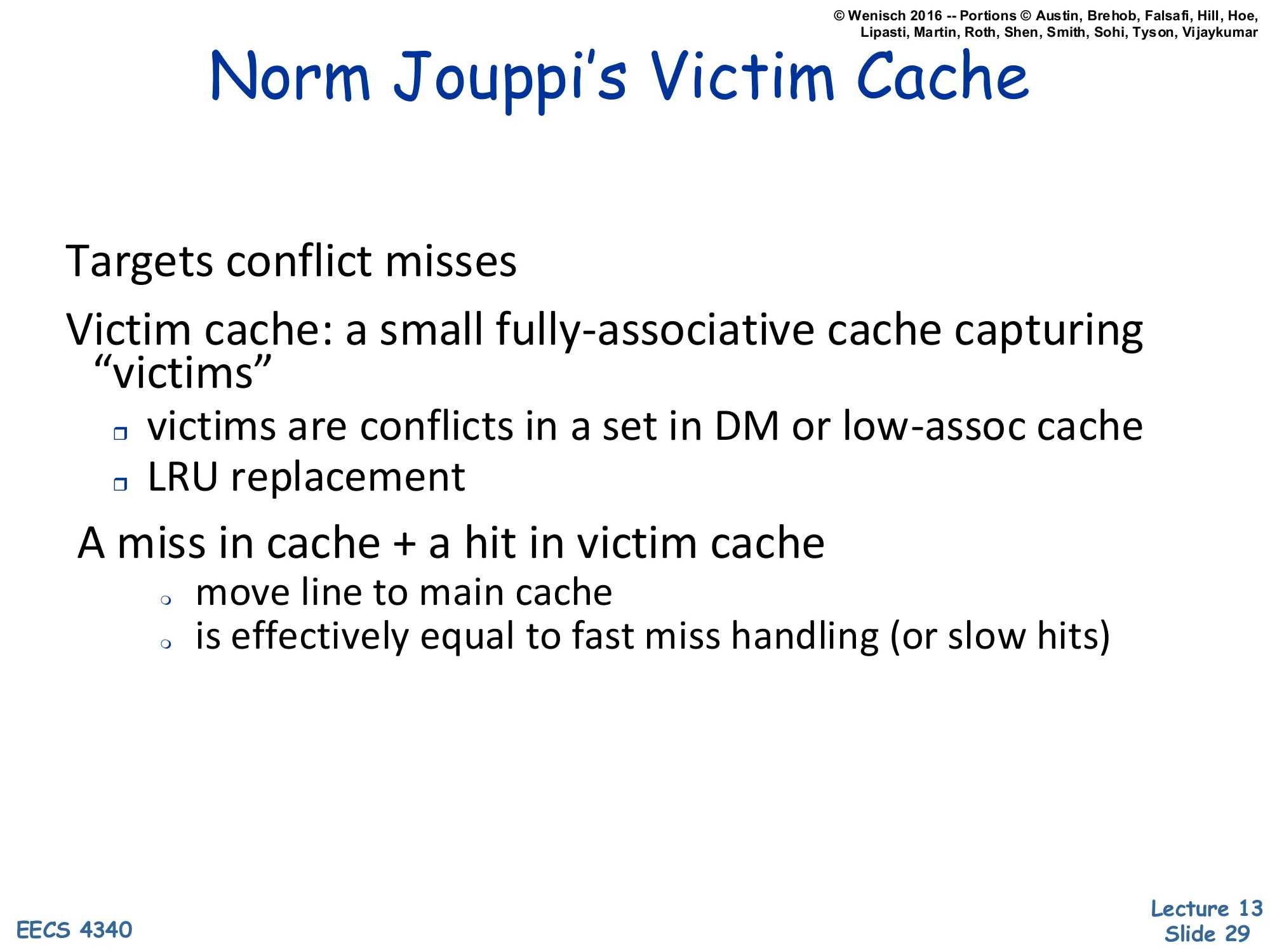
Show slide text
Norm Jouppi’s Victim Cache
Targets conflict misses
Victim cache: a small fully-associative cache capturing “victims”
- victims are conflicts in a set in DM or low-assoc cache
- LRU replacement
A miss in cache + a hit in victim cache:
- move line to main cache
- is effectively equal to fast miss handling (or slow hits)
The victim cache is target-specific: it converts conflict misses into a slow hit (one extra cycle to read the small fully-associative victim buffer). It does nothing for capacity or compulsory misses. Its small size (commonly 4–16 lines) keeps the fully-associative search cheap and makes LRU replacement trivial to implement. The mental model on the last bullet is important: a hit in the victim cache is equivalent to a miss in the main cache that is satisfied very quickly by the buffer next to it. So you can either think of it as making certain misses fast (“fast miss handling”) or as adding a tiny extra layer of slow hits — same operation, different framing. This is the conceptual ancestor of every scratchpad-buffer-next-to-cache idea, including write coalescing buffers, prefetch buffers, and stream buffers (L14).
Victim Cache's Performance
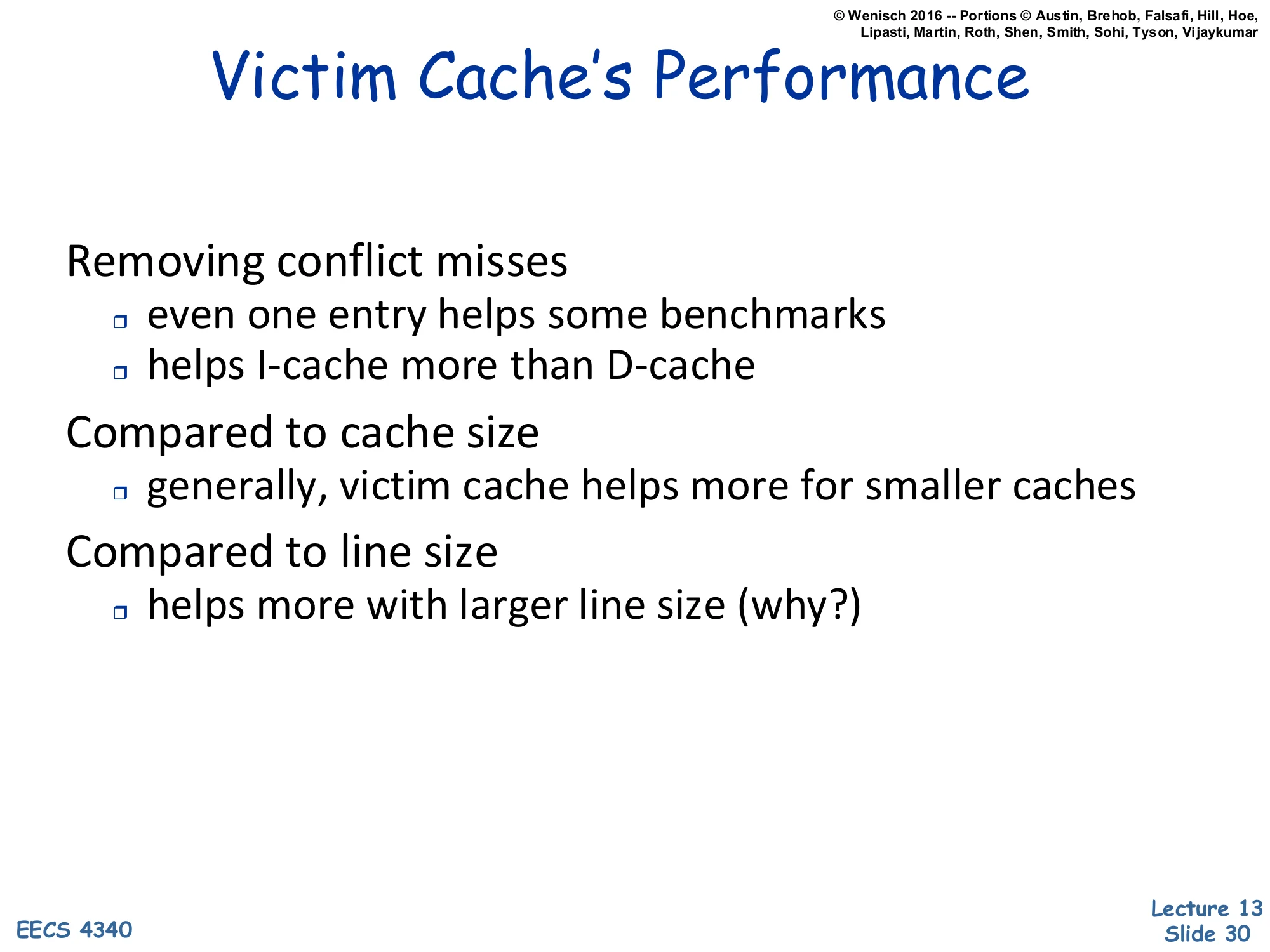
Show slide text
Victim Cache’s Performance
Removing conflict misses
- even one entry helps some benchmarks
- helps I-cache more than D-cache
Compared to cache size
- generally, victim cache helps more for smaller caches
Compared to line size
- helps more with larger line size (why?)
Empirical observations from Jouppi’s experiments. “Even one entry helps” says that ping-pongs between two mutually-conflicting addresses are surprisingly common — a 1-entry victim buffer eliminates them entirely. “I-cache more than D-cache” reflects the more deterministic structure of code — instruction streams have predictable conflict patterns (e.g., an inner loop that just barely overflows its set), while data accesses are noisier. “More for smaller caches” is intuitive: smaller caches have more conflicts, and the victim cache addresses exactly those. “Larger line size” is the trickiest claim — the rationale is that bigger lines mean fewer total lines, fewer sets, and therefore higher conflict probability per line; the victim cache rescues more of those conflict victims. Together these results explain why almost every commercial L1 has a victim-buffer-like structure (sometimes called a “miss buffer” or “writeback buffer” with slightly different semantics).
Reducing Miss Cost
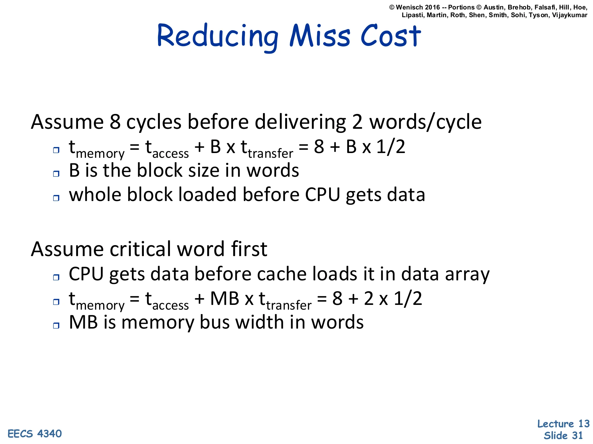
Show slide text
Reducing Miss Cost
Assume 8 cycles before delivering 2 words/cycle
- tmemory=taccess+B×ttransfer=8+B×1/2
- B is the block size in words
- whole block loaded before CPU gets data
Assume critical word first
- CPU gets data before cache loads it in data array
- tmemory=taccess+MB×ttransfer=8+2×1/2
- MB is memory bus width in words
This slide quantifies the critical-word-first optimization. Without it, the CPU stalls for the full block transfer: taccess=8 cycles to start, then B×ttransfer for B words at 2 words/cycle (so B/2 cycles). For a 16-word block, that is 8+8=16 cycles. With critical-word-first, the memory controller routes the requested word(s) to the CPU as soon as the first beat arrives, rather than refilling the line in address order; the CPU resumes after only taccess+MB×ttransfer where MB is the bus width in words (typically 2). For the same example: 8+2×1/2=9 cycles for the CPU’s data, with the rest of the line filling in the background while the CPU executes. The remaining B−MB words pose a hazard — if the CPU touches one before the line is fully filled, the cache must stall (or the line-fill engine must merge). Early restart is a slight variant — refill in order but let the CPU restart on the first word — and is the more common implementation in practice.
Large Blocks and Subblocking
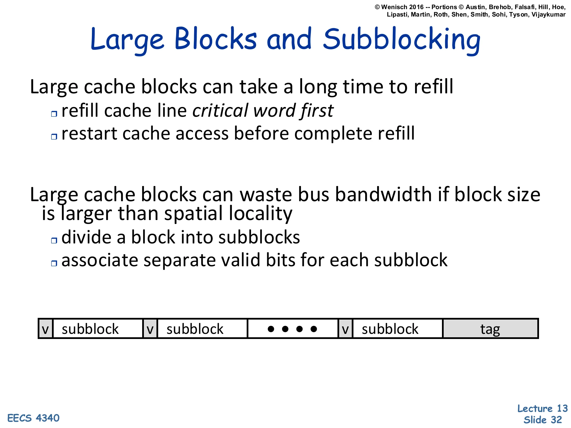
Show slide text
Large Blocks and Subblocking
Large cache blocks can take a long time to refill
- refill cache line critical word first
- restart cache access before complete refill
Large cache blocks can waste bus bandwidth if block size is larger than spatial locality
- divide a block into subblocks
- associate separate valid bits for each subblock
[Diagram: cache line = | v | subblock | v | subblock | … | v | subblock | tag |]
Large blocks reduce compulsory misses (one fetch covers many bytes of spatial locality) and amortize tag overhead, but they have two costs: long refill time and wasted bandwidth when the program does not actually use the whole line. Critical-word-first + early restart attacks the first cost (already on the previous slide). Subblocking attacks the second by adding a valid bit per sub-block (smaller than the cache line but larger than a word) — the tag still covers the whole line for snooping and address-compare purposes, but the cache only refills the subblocks the program actually touches. On a write-allocate miss, only the subblock(s) being written get refilled; the rest stay invalid until separately demanded. The diagram shows the storage layout: a single tag at the end, and a (valid, subblock) pair for each subblock. This is essentially decoupling the tag granularity (large) from the transfer/valid granularity (small) — useful especially in caches with very large lines like L3 or DRAM-backed caches.
Multi-Level Caches
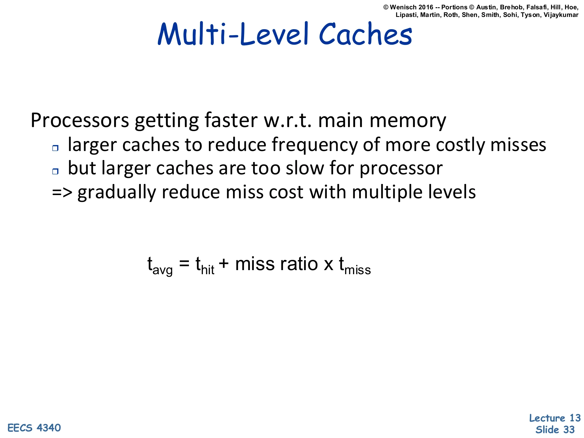
Show slide text
Multi-Level Caches
Processors getting faster w.r.t. main memory
- larger caches to reduce frequency of more costly misses
- but larger caches are too slow for processor
- ⇒ gradually reduce miss cost with multiple levels
tavg=thit+miss ratio×tmiss
The fundamental tension: bigger caches catch more misses (lower miss ratio) but have higher hit time, and processor cycles scale faster than memory cycles, so each miss is more cycles wasted as time goes on. A single cache cannot be both fast (small) and capacity-effective (large). The solution is gradual — a hierarchy of progressively larger and slower caches, each of which catches what the previous level missed. The recursive AMAT formula on the next slide captures this. The slide also implicitly motivates why we have an L2 on-die (close enough to the core to be much faster than DRAM) but separate from L1 (large enough that putting it inside L1’s tight latency budget would explode L1’s cycle time). Modern systems extend this to L3 (often shared across cores) and even L4 (eDRAM or HBM-based).
Multi-Level Cache Design
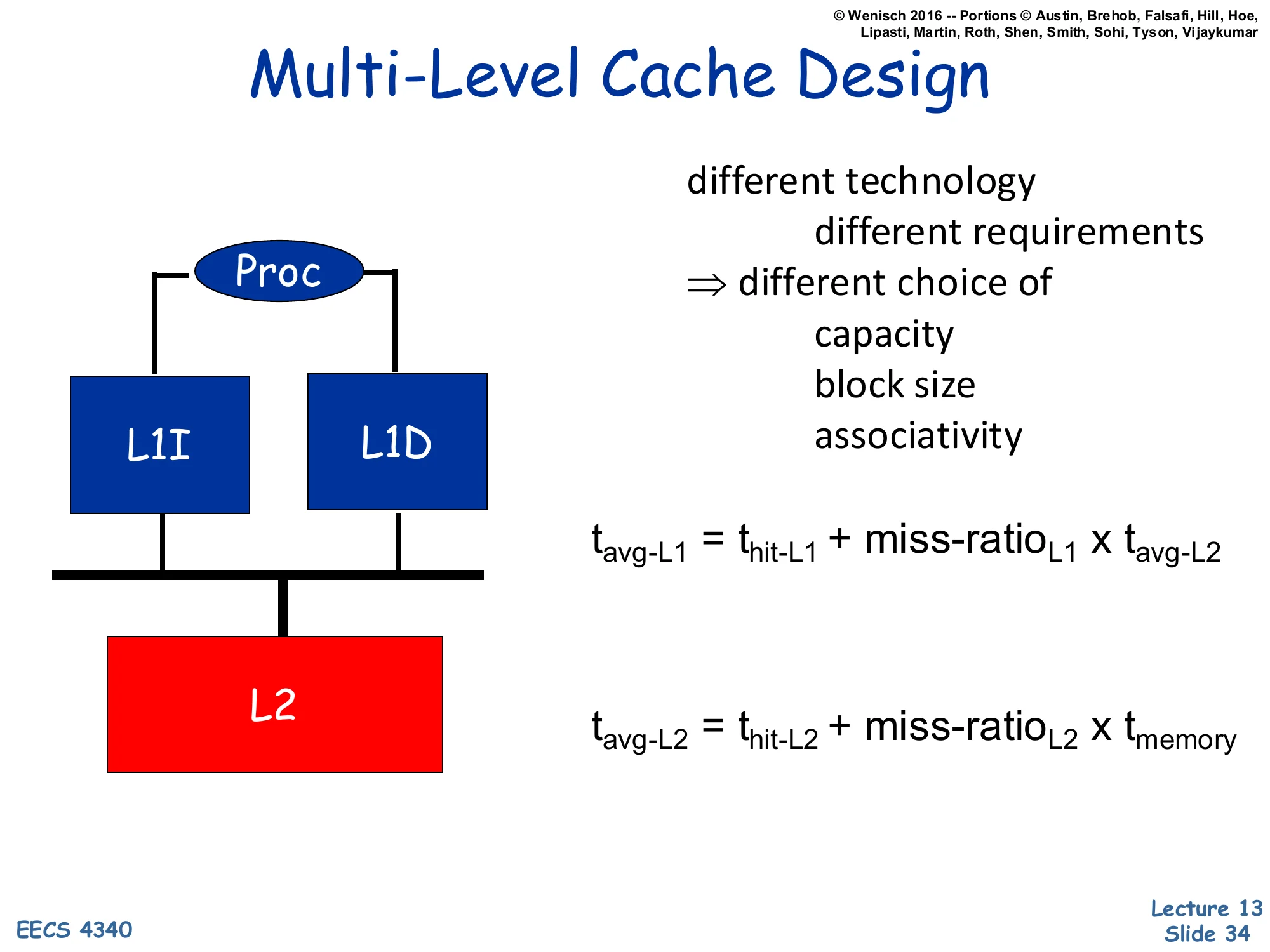
Show slide text
Multi-Level Cache Design
[Diagram: Proc → split L1I and L1D → unified L2 → memory.]
different technology, different requirements ⇒ different choice of
- capacity
- block size
- associativity
tavg−L1=thit−L1+miss-ratioL1×tavg−L2
tavg−L2=thit−L2+miss-ratioL2×tmemory
Different levels have different design constraints, so they pick different parameters. L1 is in the critical path of every load — it needs to hit in 1–4 cycles, so it is small (32–64KB), low-associativity (typically 4–8 way), and has small lines (often 64B); split into L1I and L1D so instructions and data each get a dedicated port. L2 is reached only on L1 misses (much lower bandwidth requirement), so it is unified, large (256KB–1MB per core), higher-associativity (8–16 way), and accessed in 10–15 cycles. L2 lines are sometimes the same size as L1 but can be larger. The recursive AMAT formula composes: the L1’s tmiss is the L2’s tavg, and so on down. This composition means that even a high L1 miss ratio is acceptable if L2 is fast enough — the multi-level hierarchy is more tolerant than a single level would be.
The Inclusion Property
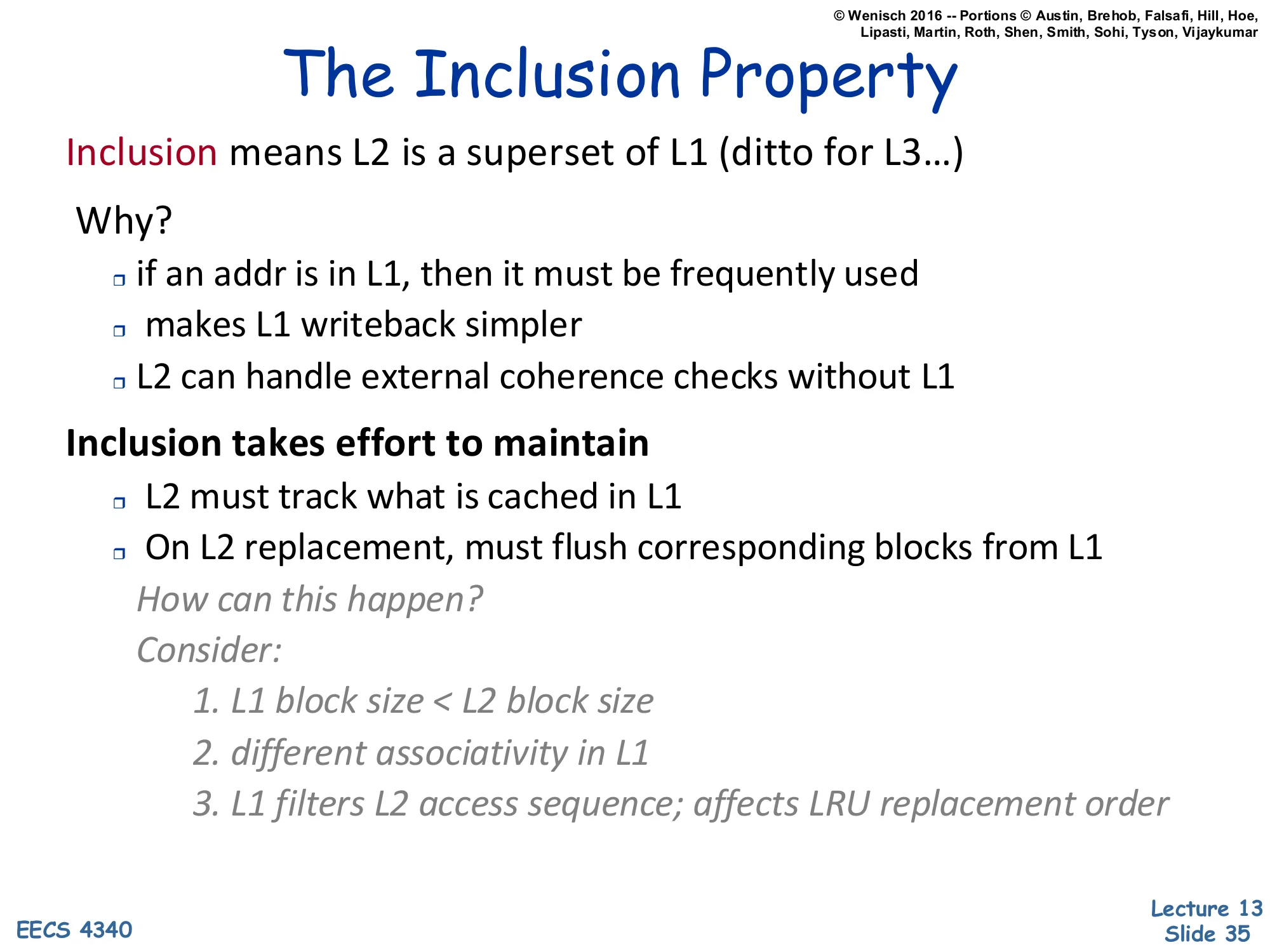
Show slide text
The Inclusion Property
Inclusion means L2 is a superset of L1 (ditto for L3…)
Why?
- if an addr is in L1, then it must be frequently used
- makes L1 writeback simpler
- L2 can handle external coherence checks without L1
Inclusion takes effort to maintain
- L2 must track what is cached in L1
- On L2 replacement, must flush corresponding blocks from L1
How can this happen? Consider:
- L1 block size < L2 block size
- different associativity in L1
- L1 filters L2 access sequence; affects LRU replacement order
Inclusion is a property — usually maintained between L1 and L2, not always between L2 and L3 — that says everything in the smaller (closer) cache is also present in the larger (farther) cache. Its main practical value is coherence simplification: an external snoop from another core or from DMA only needs to check L2; if L2 misses, L1 is guaranteed to also miss, so L1 does not need to respond to snoops at all. Inclusion is not free. L2 must remember which lines are also cached in L1 (typically with a per-line “inclusion bit” or by tracking L1 ways). When L2 evicts a line that is still in L1, the protocol must back-invalidate — flush the line from L1 — to maintain inclusion. The three reasons inclusion can break naturally are subtle: (1) different block sizes mean an L2 line maps to multiple L1 lines, so partial inclusion is possible; (2) different associativity means an address could fit in L1 but be evicted from L2 because L2’s set is full; (3) L1 filters reuse from L2’s view, so L2’s LRU bits are stale relative to actual access patterns, making it more likely to evict a line L1 still values. The next slide gives a concrete violation example.
Possible Inclusion Violation
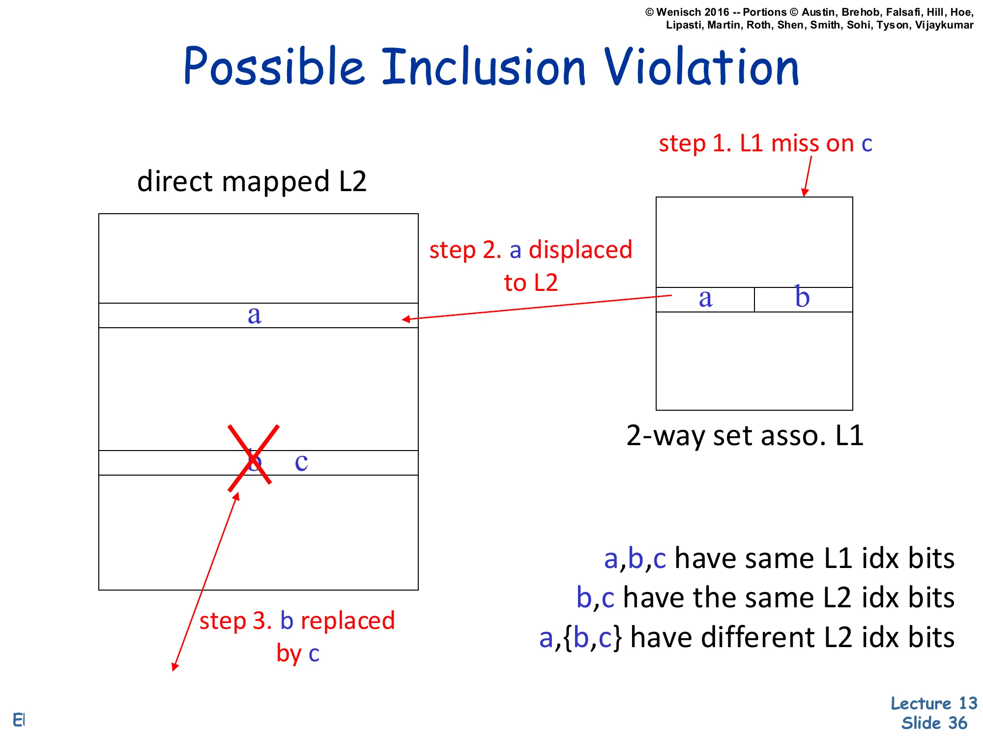
Show slide text
Possible Inclusion Violation
[Diagram: 2-way set associative L1 holds {a, b}. Direct-mapped L2 holds a; b and c map to the same L2 set.
step 1. L1 miss on c step 2. a displaced to L2 step 3. b replaced by c (in L2)]
- a, b, c have same L1 idx bits
- b, c have the same L2 idx bits
- a, {b,c} have different L2 idx bits
Concrete example of why inclusion is not automatic. Setup: L1 is 2-way set associative, L2 is direct-mapped. Addresses a,b,c all share the same L1 index (so they compete for L1’s two ways). Addresses b and c share the same L2 index (so they compete for L2’s single slot). a has a different L2 index. Step 1: a load of c misses L1; the cache fetches c from L2 (which misses too) and goes to memory. To install c in L1, one of {a,b} has to be evicted — say a. Step 2: a flows to L2, taking its own L2 slot. Step 3: c also has to install in L2; but c‘s L2 slot is occupied by b (since b,c share L2 index). b gets replaced by c in L2. Now b is in L1 but not in L2 — inclusion is violated. Without explicit back-invalidation, the system would silently violate inclusion and break the snoop-only-L2 invariant. Modern processors avoid this by either back-invalidating b from L1 when b is evicted from L2, or by relaxing inclusion to exclusion / non-inclusive. The diagram is dense but legible — the three labeled steps are the load-bearing content.
Multi-Level Inclusion (Cont.)
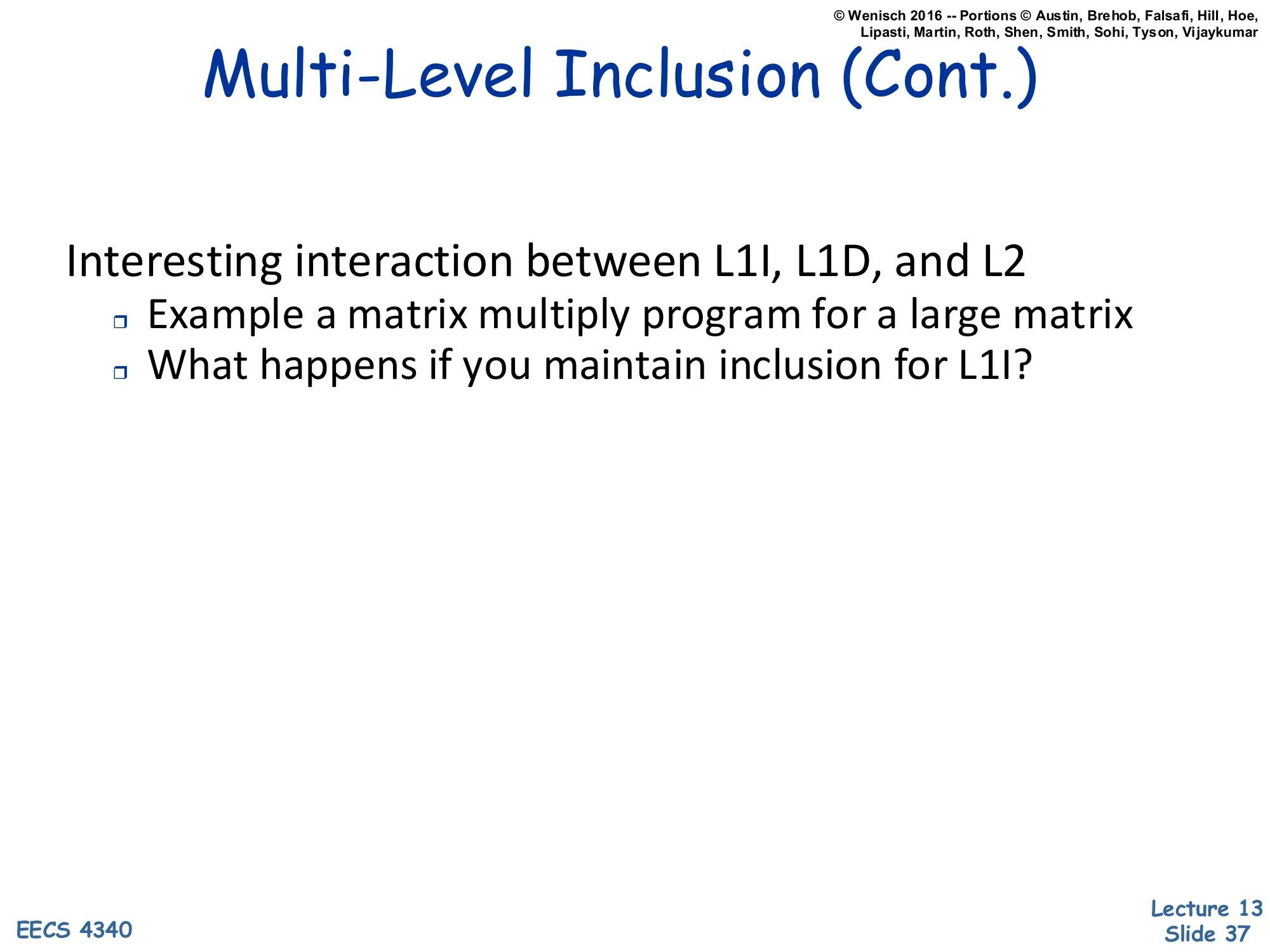
Show slide text
Multi-Level Inclusion (Cont.)
Interesting interaction between L1I, L1D, and L2
- Example a matrix multiply program for a large matrix
- What happens if you maintain inclusion for L1I?
The hidden trap with inclusion is the combined footprint of L1I and L1D. L2 must include everything in both L1 caches. Consider a large matrix multiply: the inner loop’s instruction footprint is small (a few cache lines of code) but the data footprint is enormous (the matrices). The L2 has to hold both — and on L2 evictions, it can accidentally back-invalidate hot instruction lines from L1I if data evictions force the inner-loop’s code lines out of L2. This produces pathological I-cache miss bursts in the middle of compute kernels. The fix is either partial inclusion (only data, not instructions) or simply over-provisioning L2 relative to the combined L1I+L1D size (the typical ≥8× rule on the next slide). This is a real-world example of why “L2 ≥ 8× L1” is not just folklore — it is a buffer to keep code lines safe from data-induced evictions.
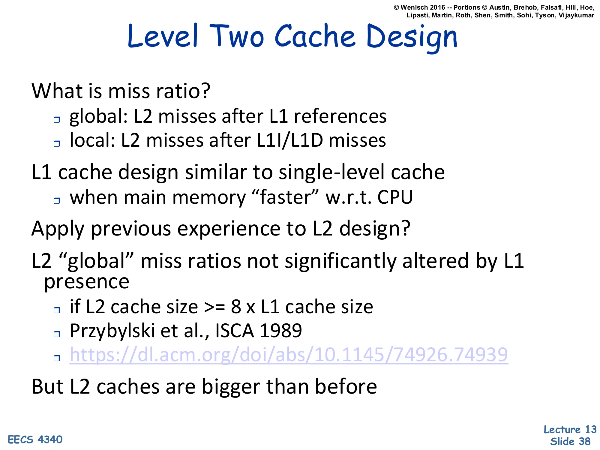
Level Two Cache Design
Show slide text
Level Two Cache Design
What is miss ratio?
- global: L2 misses after L1 references
- local: L2 misses after L1I/L1D misses
L1 cache design similar to single-level cache
- when main memory “faster” w.r.t. CPU
Apply previous experience to L2 design?
L2 “global” miss ratios not significantly altered by L1 presence
- if L2 cache size >= 8 × L1 cache size
- Przybylski et al., ISCA 1989
- https://dl.acm.org/doi/abs/10.1145/74926.74939
But L2 caches are bigger than before
Two miss-rate definitions are used in multi-level analysis. Local miss rate is L2-misses / L2-accesses — informative for L2 designers but misleading because it only counts the small fraction of references that already missed L1 (so a high local rate can still mean a low global rate). Global miss rate is L2-misses / total-CPU-references — the meaningful number for system performance. The Przybylski result is the foundation of the “L2 should be at least 8× L1” rule of thumb: when L2 is at least 8× larger, L1’s filtering of access streams does not significantly change L2’s global miss rate compared to a single-level cache of the same total size. This decouples L2 design from L1 design, letting them be tuned independently. The closing note — “L2 caches are bigger than before” — is a reminder that modern L2s (256KB–1MB) far exceed L1 (32–64KB) by 8–16×, so the rule’s preconditions are typically satisfied.
Emerging Technology: 3D Stacking
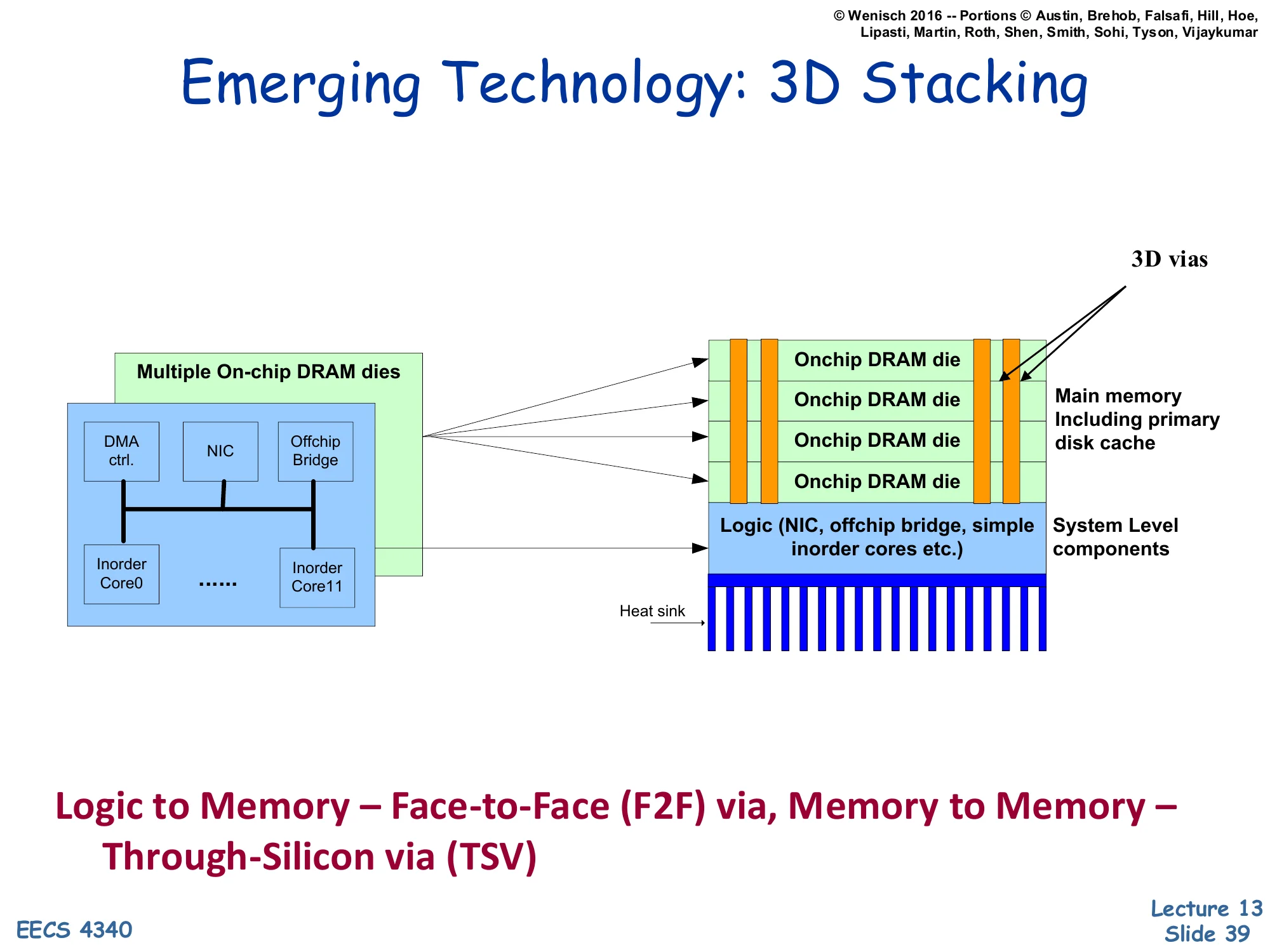
Show slide text
Emerging Technology: 3D Stacking
[Diagram: a logic die (cores, DMA controller, NIC, off-chip bridge) with multiple on-chip DRAM dies stacked on top, connected by 3D vias (TSVs). The logic-to-memory connection is a face-to-face (F2F) via; memory-to-memory is through-silicon via (TSV). A heat sink sits below.]
Logic to Memory — Face-to-Face (F2F) via, Memory to Memory — Through-Silicon via (TSV)
3D-stacked memory packages multiple DRAM dies on top of (or face-to-face with) the logic die using through-silicon vias (TSVs) — vertical conductors that punch through the silicon. The connection density is dramatically higher than off-chip pins (thousands of TSVs vs. ~1000 pins), which means much higher memory bandwidth and lower per-bit energy. Logic-to-memory bonds are typically face-to-face for the highest density and shortest latency; memory-to-memory bonds use TSVs to chain stacked layers. Real implementations include HBM (High Bandwidth Memory, used in GPUs), Hybrid Memory Cube, and Intel’s Foveros packaging. From a cache-architect viewpoint, 3D stacking creates the possibility of very large on-package caches (hundreds of MB) that act like a fast L4. The thermal challenge is real — DRAM is sensitive to temperature, and stacking it on a hot logic die requires careful heat-sink design (visible at the bottom of the diagram).
Non-blocking Caches
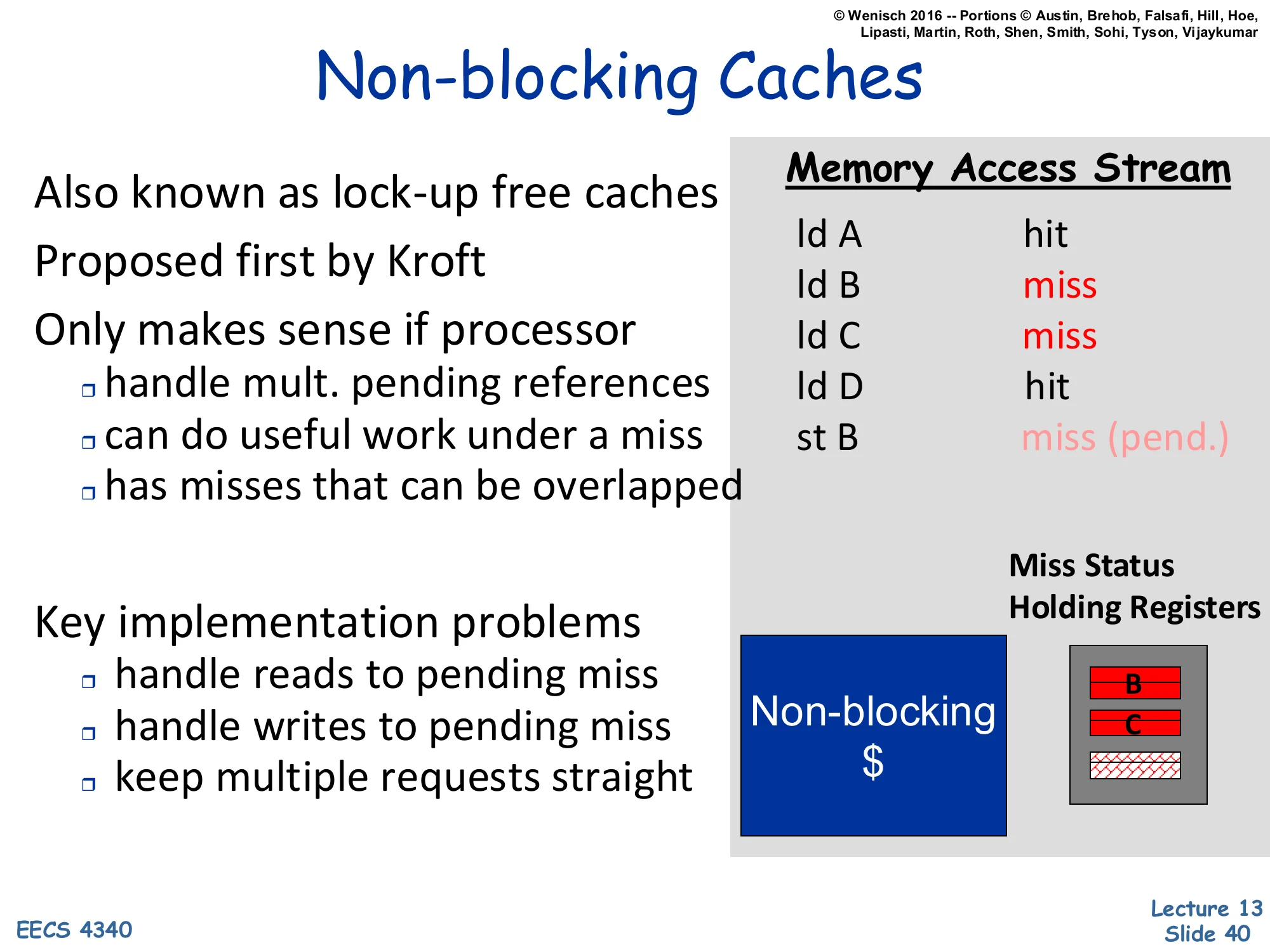
Show slide text
Non-blocking Caches
Also known as lock-up free caches Proposed first by Kroft
Only makes sense if processor:
- handle mult. pending references
- can do useful work under a miss
- has misses that can be overlapped
Key implementation problems:
- handle reads to pending miss
- handle writes to pending miss
- keep multiple requests straight
Memory Access Stream
- ld A — hit
- ld B — miss
- ld C — miss
- ld D — hit
- st B — miss (pend.)
[Diagram: Non-blocking $ holds Miss Status Holding Registers tracking outstanding lines B and C.]
A blocking cache stalls completely on a miss — every later access waits behind the first miss. A non-blocking (lock-up-free) cache continues servicing subsequent accesses while earlier misses are pending. This only matters for cores that can themselves continue under a miss: out-of-order execution, store buffers, or non-blocking I/O. Three implementation problems must be solved. Reads to a pending miss line — the cache must recognize the duplicate request and merge it with the outstanding miss rather than issuing a second memory request. Writes to a pending miss line — the write must be merged into the line being filled, with byte-mask tracking so partial fills are correct. Multiple in-flight requests — the responses can come back out of order, so each request must be tagged. The data structure that does all this is the MSHR (Miss Status Holding Register), shown holding entries for B and C in the diagram. The trace in the slide illustrates: A hits, B misses (allocate MSHR), C misses (allocate another MSHR), D hits independently, then a store to B finds B’s MSHR and merges in. Non-blocking caches are essential for any modern OoO core with even moderate memory-level parallelism.
Lock-up Free Caches (Cont.)
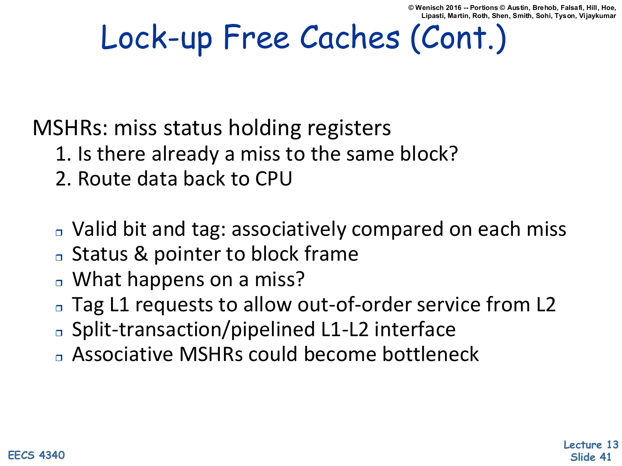
Show slide text
Lock-up Free Caches (Cont.)
MSHRs: miss status holding registers
- Is there already a miss to the same block?
- Route data back to CPU
- Valid bit and tag: associatively compared on each miss
- Status & pointer to block frame
- What happens on a miss?
- Tag L1 requests to allow out-of-order service from L2
- Split-transaction/pipelined L1-L2 interface
- Associative MSHRs could become bottleneck
MSHRs are the workhorse of any non-blocking cache. Each MSHR entry holds the block address (compared associatively against incoming misses to detect duplicates) plus status (waiting, returning, etc.) and a pointer to where the line will be installed. On a new miss, the MSHR file is searched: a hit means “already in flight” — record the request as a sub-entry on the existing MSHR; a miss allocates a new MSHR and dispatches the memory request. The L1-L2 interface must be split-transaction (request and response are decoupled and tagged) so multiple requests can be in flight simultaneously. The number of MSHRs upper-bounds the cache’s memory-level parallelism — more MSHRs allow more outstanding misses, supporting wider OoO cores and more aggressive prefetching. The associative search of MSHRs becomes a bottleneck at scale; large designs use multi-bank MSHR files or coarser hashing. Modern Intel cores have 10–16 L1D MSHRs; the L2 has even more, and the LLC has hundreds.
Latency vs. Bandwidth
Show slide text
Latency vs. Bandwidth
Latency can be handled by:
- hiding/tolerating techniques
- e.g., parallelism
- may increase bandwidth demand
- reducing techniques
Ultimately limited by physics
Latency and bandwidth are the two memory-system metrics; they trade off. Latency is the wall-clock time of a single access; bandwidth is the sustained throughput. Hiding latency means doing other work while a miss is outstanding — out-of-order execution, prefetching, multithreading — none of these reduce per-access latency, they overlap it with useful work. Crucially, hiding latency increases bandwidth demand: more outstanding misses means more concurrent transfers in flight. Reducing latency means making the access itself faster — bigger/faster caches, lower cycle counts, technology improvements. The physics floor is the speed of light through the wires plus the access time of the SRAM/DRAM cells; once you are at that floor, only architectural overlap can hide the residual. Modern L1 latency is ~1ns (4 cycles at 4GHz), close to physics; DRAM is ~50–100ns and improving slowly because the row-cycle time is bounded by sense-amp and bitline physics.
Latency vs. Bandwidth (Cont.)
Show slide text
Latency vs. Bandwidth (Cont.)
Bandwidth can be handled by:
- banking/interleaving/multiporting
- wider buses
- hierarchies (multiple levels)
What happens if average demand not supplied?
- bursts are smoothed by queues
- if burst is much larger than average ⇒ long queue
- eventually increases delay to unacceptable levels
Bandwidth, in contrast to latency, scales fairly directly with parallel hardware: split the cache into banks (each accessible in parallel), widen the bus (more bytes per cycle), or add levels so the lower level handles fewer requests per second. Each technique adds area or complexity but yields bandwidth in proportion. The closing note is the queueing-theory caveat: if demand exceeds capacity, queues build up; by Little’s law, the queue length equals arrival-rate × waiting-time, so as utilization approaches 100% the queueing time grows unboundedly. Real systems must run below ~70% utilization to keep tail latency bounded. This is why a cache that is “barely able” to supply average bandwidth has terrible burst behavior — and why over-provisioning bandwidth at every level (with extra ports, FIFOs, etc.) is essential.
Issue Bandwidth
Show slide text
Issue Bandwidth
Increasing issue width ⇒ wider caches
Parallel cache access is harder than parallel FUs
- fundamental difference: caches have state, FUs don’t
- one port affects future for other ports
Several approaches used:
- true multi-porting
- multiple cache copies
- virtual multi-porting
- multi-banking (interleaving)
- line buffers
A wide superscalar processor issues multiple loads/stores per cycle, so its L1 cache must serve multiple references simultaneously. The fundamental difficulty: caches are stateful — a port that updates the cache (via a fill, a store, or a replacement) affects what other ports see, so concurrent ports must coordinate. Function units (adders, multipliers) are stateless (or only have register-file state) and can simply be replicated. The five techniques on the slide are the entire design space for cache bandwidth, expanded over the next several slides: true multi-porting (genuinely multi-ported SRAMs — expensive), multiple cache copies (replicate the array per port — area-doubling), virtual multi-porting (time-multiplex one port at higher frequency), multi-banking (split the cache by address into banks and serve different banks in parallel), and line buffers (small per-port latches that capture recently-fetched lines for repeated access).
Multi-Port Caches: True Multiporting
Show slide text
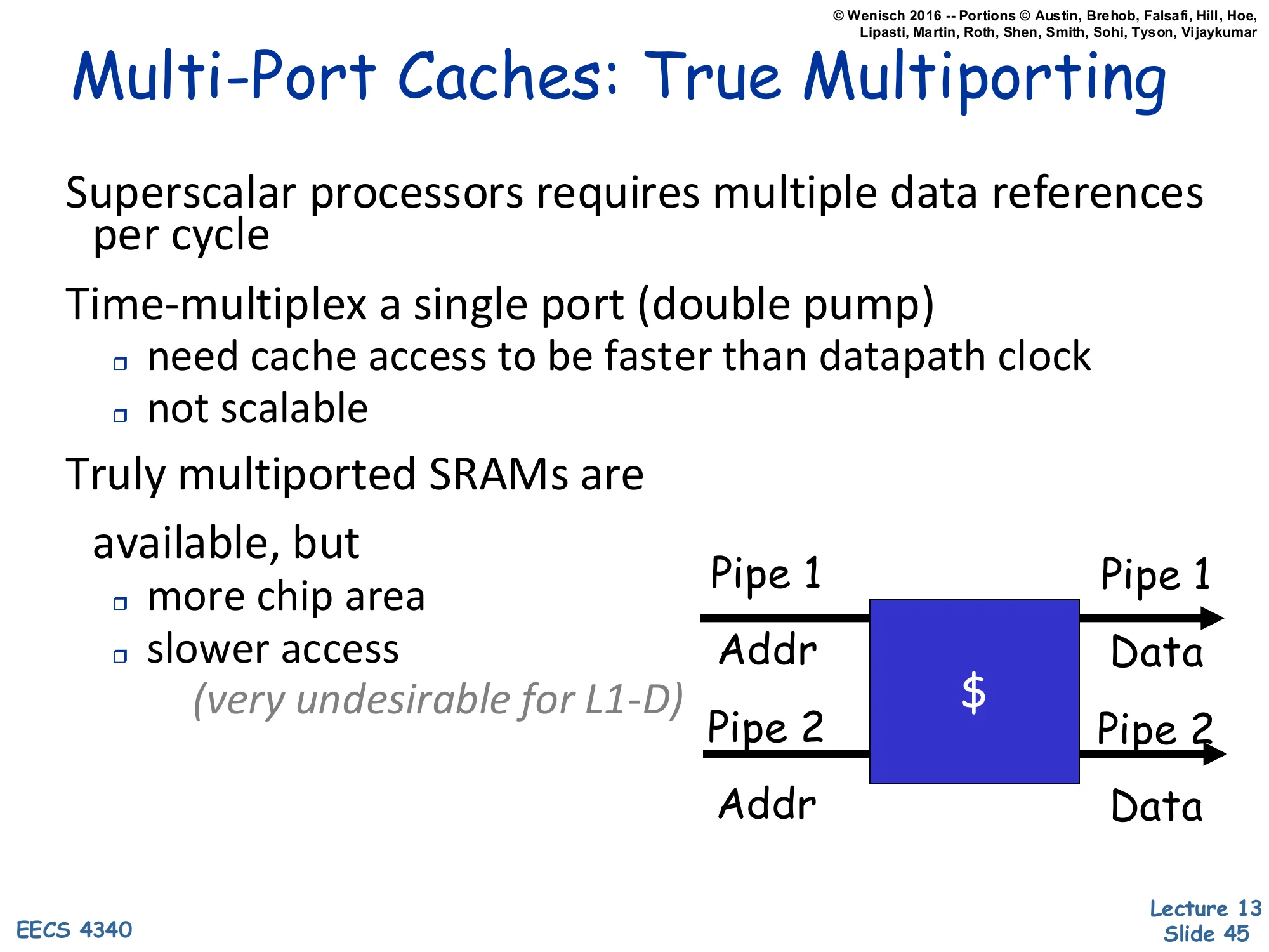
Multi-Port Caches: True Multiporting
Superscalar processors requires multiple data references per cycle
Time-multiplex a single port (double pump)
- need cache access to be faster than datapath clock
- not scalable
Truly multiported SRAMs are available, but
- more chip area
- slower access (very undesirable for L1-D)
[Diagram: $ with two address inputs (Pipe 1 Addr, Pipe 2 Addr) and two data outputs (Pipe 1 Data, Pipe 2 Data).]
True multi-porting means the SRAM cell itself has two read/write ports — physically two pairs of word/bit lines per cell. The benefits are obvious: two independent accesses per cycle with no conflicts. The costs are severe: each port adds a transistor pair to every cell, blowing up area roughly 1.5–2× per port and increasing capacitance on the bitlines, which slows access and raises power. The slide’s note “very undesirable for L1-D” reflects that L1-D is the most timing-critical structure on the chip — any latency increase ripples into pipeline depth. Time-multiplexing (“double pumping”) is a poor-man’s alternative: clock the cache at 2× the datapath rate and serve two requests per datapath cycle. This requires a fast SRAM and is not scalable beyond 2 (and increasingly hard at high core frequencies). True multi-porting is more common in register files (which are very small and benefit from the low latency) than in caches.
Virtual Multi-Porting
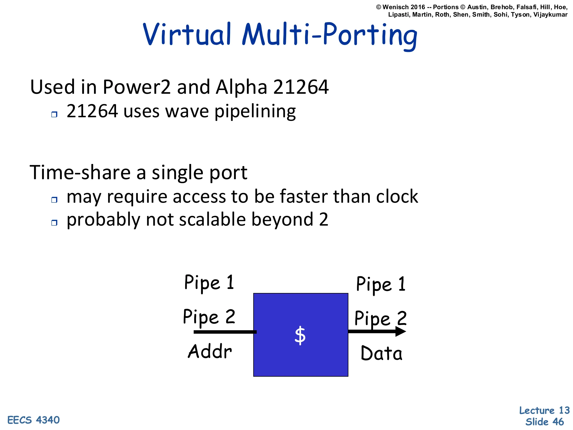
Show slide text
Virtual Multi-Porting
Used in Power2 and Alpha 21264
- 21264 uses wave pipelining
Time-share a single port
- may require access to be faster than clock
- probably not scalable beyond 2
[Diagram: $ with single port; Pipe 1 and Pipe 2 share the same Addr/Data wires by time-multiplexing.]
Virtual multi-porting is the time-multiplexing approach taken seriously: a single physical port serves multiple logical pipes by alternating cycles. The Alpha 21264 used wave pipelining — overlapping accesses through the SRAM so that two accesses are in flight at slightly different stages, requiring careful timing analysis but no extra hardware. The key constraint is that the cache must complete an access faster than the processor cycle, so the design has timing margin to fit two phases per cycle. Beyond 2, the timing margins evaporate. The diagram is a single-port cache labeled with two pipe inputs to indicate they share the wires; visually it is just a cache with an arrow and the word “Pipe 1”/“Pipe 2” labels. This is a low-cost technique (no area penalty) but with very limited scalability — it was a footnote even in its heyday.
Multiple Cache Copies
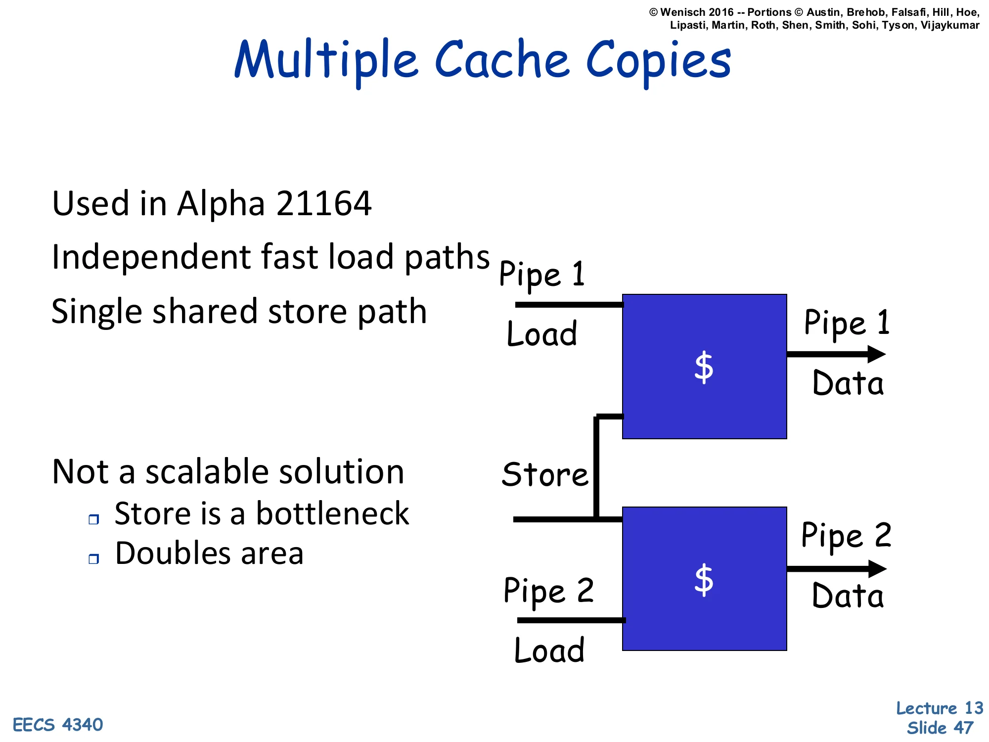
Show slide text
Multiple Cache Copies
Used in Alpha 21164
- Independent fast load paths
- Single shared store path
Not a scalable solution:
- Store is a bottleneck
- Doubles area
[Diagram: Two complete cache copies. Pipe 1 Load → →Pipe1Data;Pipe2Load→ → Pipe 2 Data. A single Store path goes to both copies (so they stay coherent).]
An aggressive area-trade approach: just replicate the entire L1 cache. Each pipe gets its own complete copy with its own dedicated load port. Loads run completely independently (full bandwidth), but stores must update both copies to keep them coherent — so the store path is shared and serializes. This was used in the Alpha 21164 to get two-load-per-cycle throughput from a 1-ported SRAM technology. The downsides are obvious: doubling the L1D area (which was a significant fraction of the die budget even in 1995), and the store path becomes the bottleneck in store-heavy code. Modern caches don’t use this approach because banking (next slide) gives better scaling at lower area, and store-heavy workloads are common enough that the store bottleneck is unacceptable. The diagram clearly labels two cache blocks with separate Load paths and a shared Store wire connecting them.
Multi-Banking (Interleaving) Caches
Show slide text
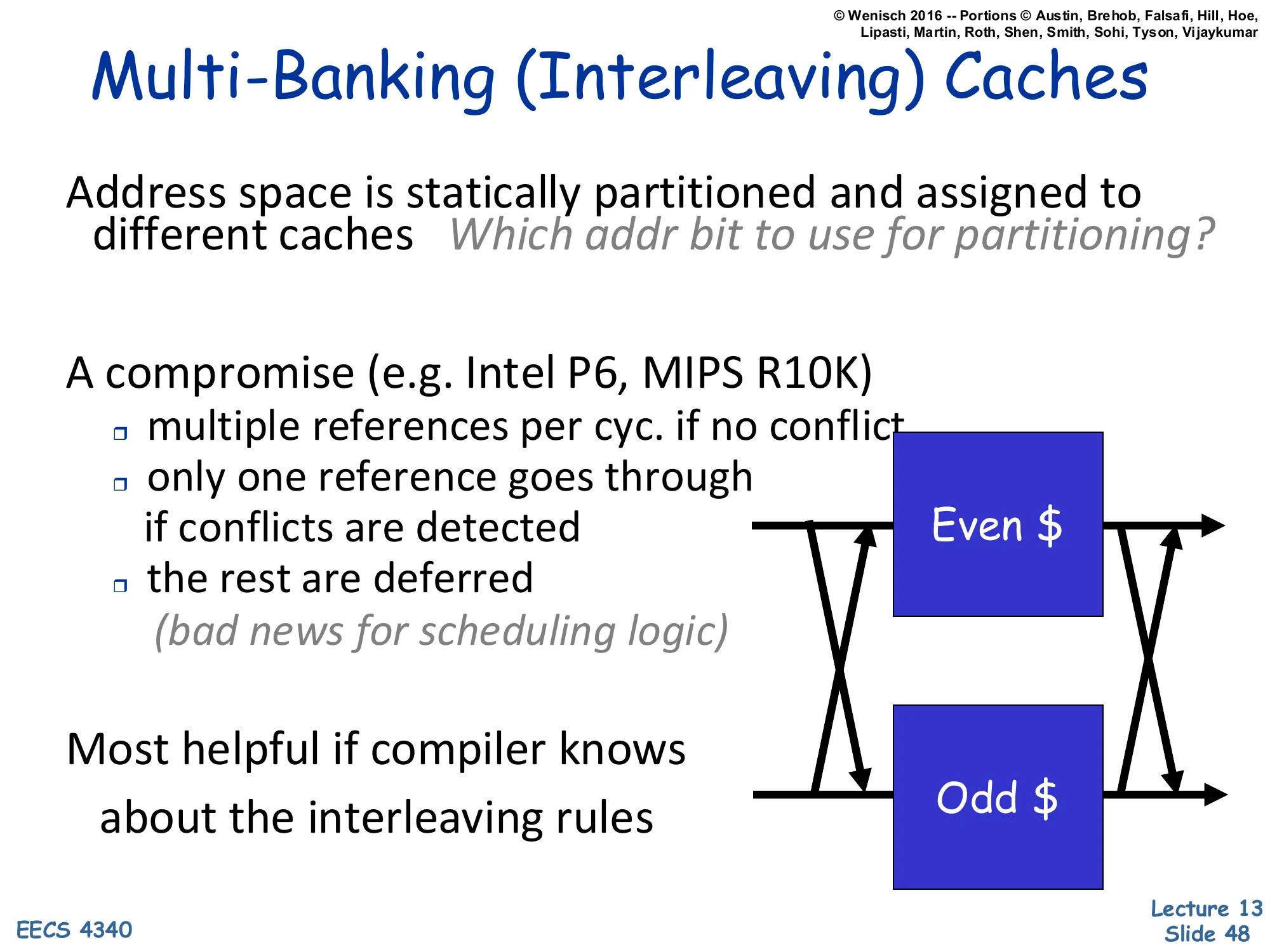
Multi-Banking (Interleaving) Caches
Address space is statically partitioned and assigned to different caches. Which addr bit to use for partitioning?
A compromise (e.g. Intel P6, MIPS R10K):
- multiple references per cyc. if no conflict
- only one reference goes through if conflicts are detected
- the rest are deferred (bad news for scheduling logic)
Most helpful if compiler knows about the interleaving rules
[Diagram: a crossbar between Pipe inputs and two banks (“Even "and"Odd”), so requests are routed by an address bit to one bank or the other.]
Multi-banking (a.k.a. interleaved cache) splits the cache into N banks, each of which can serve one access per cycle. Addresses are partitioned by some bit (or hash) — the canonical choice is the lowest non-block-offset bit, which gives even/odd interleaving. If two pipes hit different banks in the same cycle, both proceed; if they conflict on the same bank, one is deferred (and the OoO scheduler must replay it). This gives near-multi-port bandwidth at near-single-port area, as long as bank conflicts are rare. The choice of partitioning bit matters: low-order bits (interleaving by cache line) maximize bank diversity for sequential access; higher-order bits (interleaving by page) help if threads work on different pages. The compiler can sometimes help by ensuring that simultaneous accesses target different banks (e.g., when scheduling two loads in the same VLIW slot). Used in the Intel P6 and MIPS R10K — and in essentially every modern L2/L3 cache, which is heavily multi-banked.
Line Buffers (L0)
Show slide text
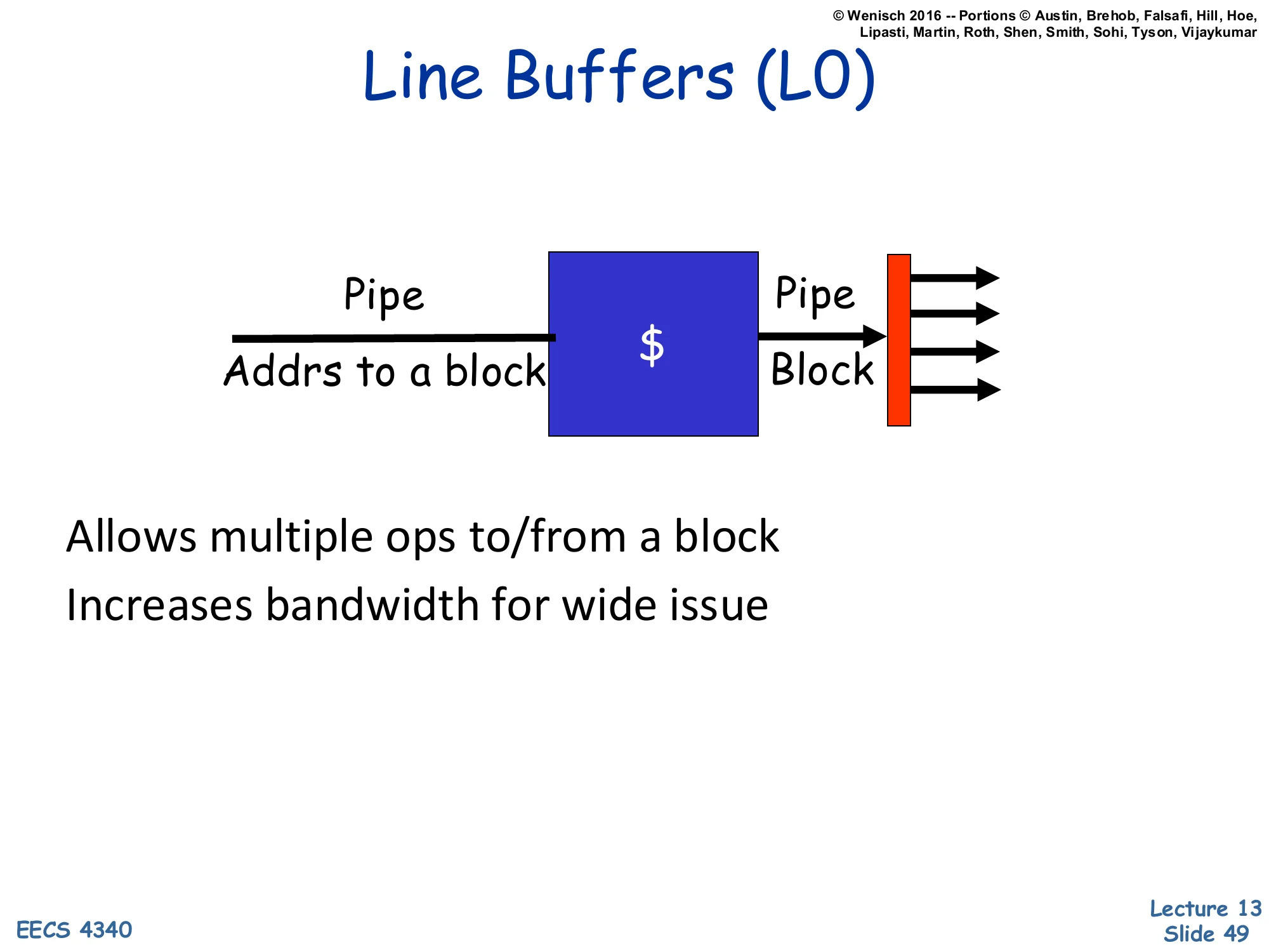
Line Buffers (L0)
[Diagram: Pipe Addrs to a block → $ → Pipe Block → red latch → multiple output paths.]
Allows multiple ops to/from a block
Increases bandwidth for wide issue
Line buffers (sometimes called L0 caches or fill buffers) are tiny (1–4 entries) latches that hold the most-recently-accessed cache line near the issue ports. When several pipes need data from the same line in the same or successive cycles, they all read the latch instead of the SRAM. Because cache lines are typically 64B (8–16 words), and successive accesses often hit the same line, the latch absorbs a lot of the bandwidth demand without burdening the cache itself. The diagram shows a single cache producing a block into a red latch that fans out to multiple output paths. This is essentially the bandwidth-amplification version of a victim cache — small dedicated structures next to the cache that hide architectural inadequacies. Used in many modern designs as fill buffers, miss buffers, and L0 storage.
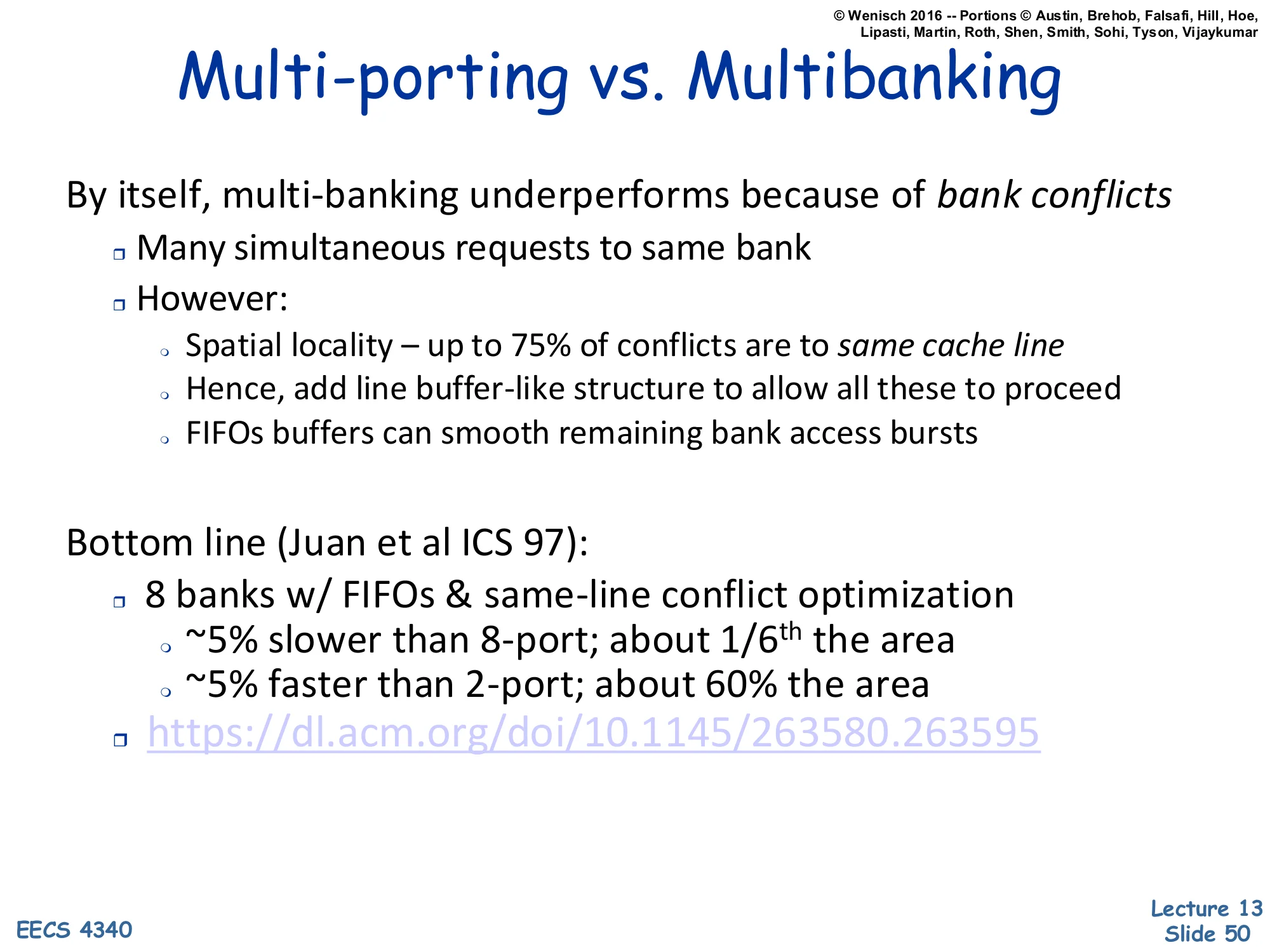
Multi-porting vs. Multibanking
Show slide text
Multi-porting vs. Multibanking
By itself, multi-banking underperforms because of bank conflicts
- Many simultaneous requests to same bank
- However:
- Spatial locality — up to 75% of conflicts are to same cache line
- Hence, add line buffer-like structure to allow all these to proceed
- FIFOs buffers can smooth remaining bank access bursts
Bottom line (Juan et al ICS 97):
- 8 banks w/ FIFOs & same-line conflict optimization
- ~5% slower than 8-port; about 1/6th the area
- ~5% faster than 2-port; about 60% the area
- https://dl.acm.org/doi/10.1145/263580.263595
This synthesis slide weighs the two main bandwidth approaches. Naive multi-banking loses to multi-porting on workloads with bursty same-bank accesses (bank conflicts force serialization). But — Juan et al. showed that 75% of bank conflicts are actually to the same cache line (because of spatial locality), so a line-buffer-like structure that catches them removes the bulk of the cost. The remaining bursts can be smoothed by per-bank FIFOs (queueing requests instead of stalling). With these two enhancements, an 8-bank cache is only ~5% slower than a true 8-port cache while occupying about 1/6 the area — a huge win. Compared to a more economical 2-port design, the 8-bank structure is even faster (5% better) and only 60% larger. This is why every modern multi-port cache uses banking + line buffers + FIFOs rather than true multi-porting: the area/perf trade-off is decisive.
Non-Uniform Cache Architecture
Show slide text
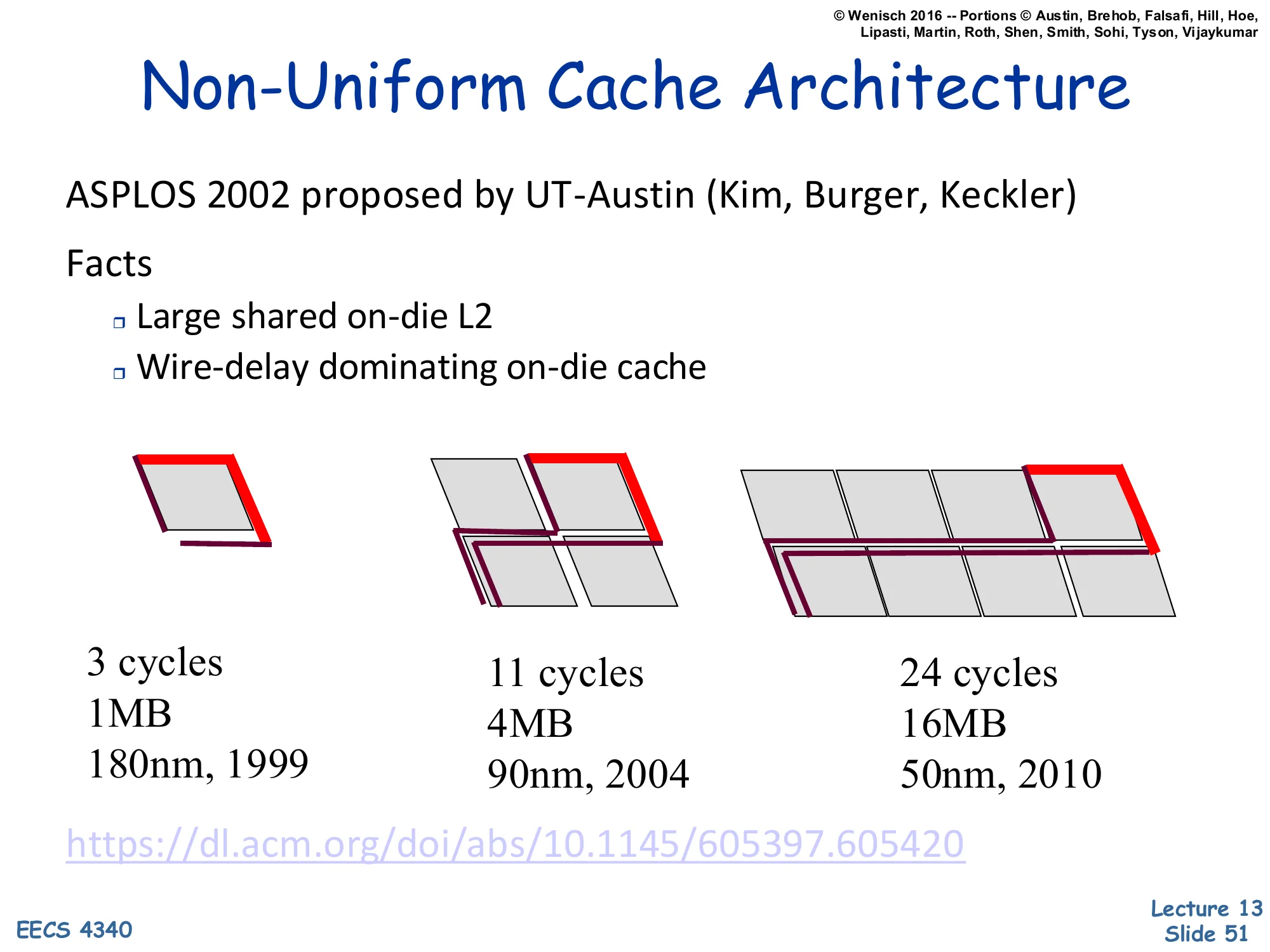
Non-Uniform Cache Architecture
ASPLOS 2002 proposed by UT-Austin (Kim, Burger, Keckler)
Facts:
- Large shared on-die L2
- Wire-delay dominating on-die cache
[Three rendered chip floorplans showing L2 cache growth over technology generations:
- 1MB at 180nm (1999) — 3 cycles
- 4MB at 90nm (2004) — 11 cycles
- 16MB at 50nm (2010) — 24 cycles]
NUCA (Non-Uniform Cache Architecture) is the big-cache analog of NUMA: when an on-die cache is physically large, the wire delay from the core to a far-corner bank dominates the SRAM access time. The slide’s data illustrates the trend: from 1999 to 2010, L2 grew 16× (1→16MB) while latency grew 8× (3→24 cycles), even though SRAM cell access time is roughly constant. Most of those 24 cycles are wires, not bitlines. The Kim/Burger/Keckler 2002 paper introduced NUCA as the response: instead of designing a single uniform-latency cache, accept that different banks have different latencies and let the architecture exploit that — closer banks should hold hotter data. The next slides show the static (S-NUCA) and dynamic (D-NUCA) variants, plus the mapping policies that decide where data lives.
Multi-banked L2 cache (2MB at 130nm)
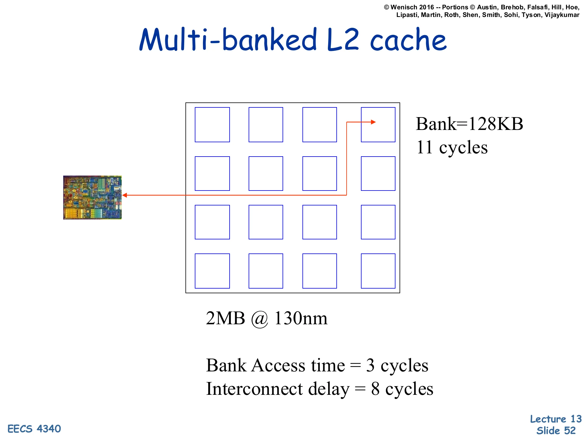
Show slide text
Multi-banked L2 cache
[Diagram: A grid of 4×4 = 16 banks, each 128KB; the CPU is at one corner. An access to the far corner takes 11 cycles total.]
2MB @ 130nm
Bank Access time = 3 cycles Interconnect delay = 8 cycles
Concrete numbers for a 2MB L2 at 130nm. The cache is sliced into 16 banks of 128KB each, and the CPU sits at one corner. The total access time is 11 cycles — but only 3 of those are bank access (the actual SRAM read), and 8 are interconnect delay (driving the address across the on-die bus to the bank, then driving the data back). For a small modern cache this is a small wire-delay fraction; the next slide shows what happens when caches grow larger. The diagram is a labeled 4×4 grid with the chip thumbnail at one corner and an arrow indicating the worst-case access path; it is reasonably legible at original resolution.
Multi-banked L2 cache (16MB at 50nm)
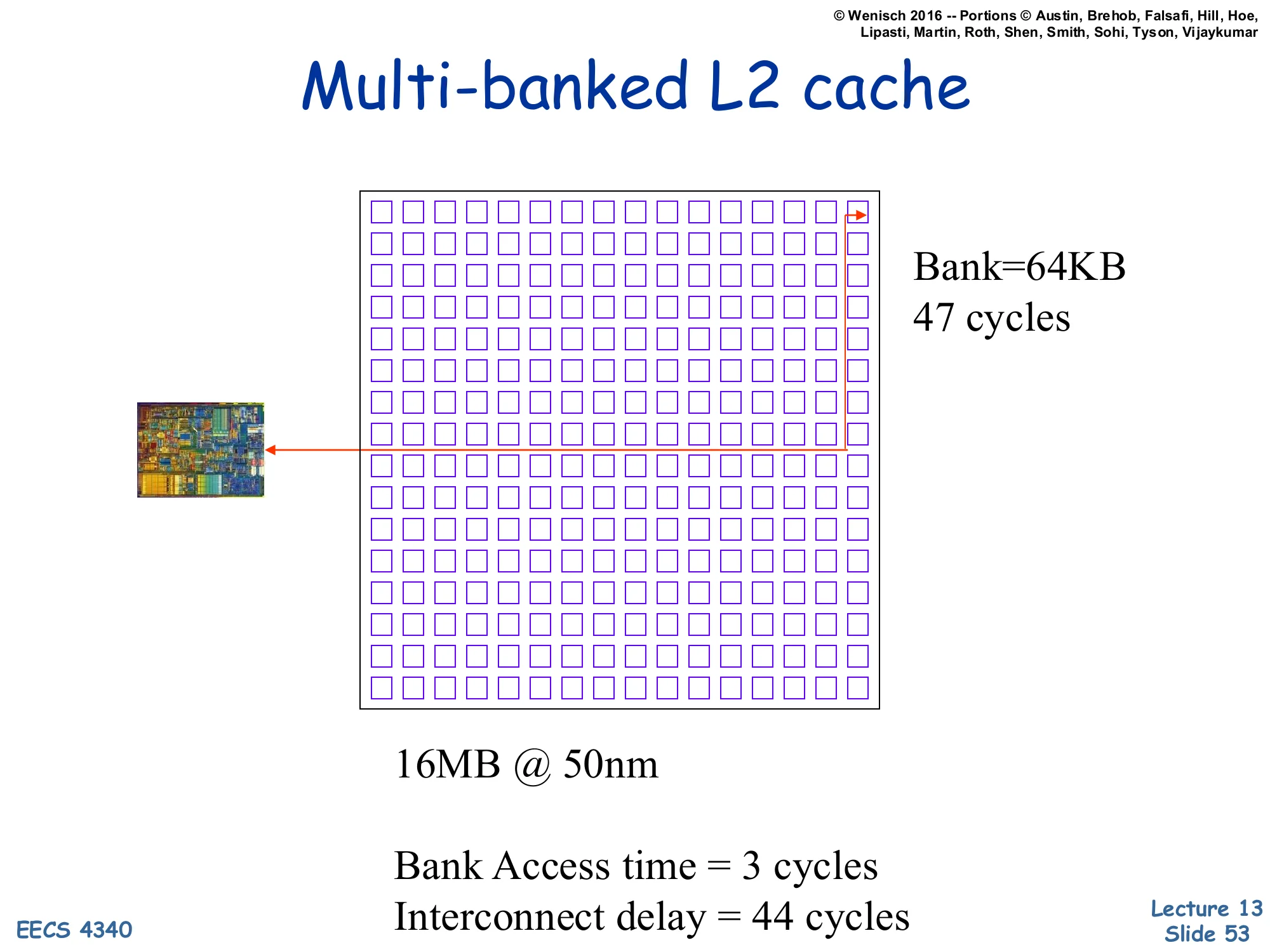
Show slide text
Multi-banked L2 cache
[Diagram: A much denser grid — 16×16 = 256 banks, each 64KB; the CPU is at one corner. Worst-case access reaches 47 cycles.]
16MB @ 50nm
Bank Access time = 3 cycles Interconnect delay = 44 cycles
By 50nm, a 16MB L2 has 256 banks of 64KB each — but the bank access time is still 3 cycles. The interconnect delay has exploded to 44 cycles, dominating the 47-cycle total. That is the wire-delay crisis — over 90% of the access time is just moving bits across the chip. A uniform cache must report 47 cycles for every access, even for nearby banks (which physically only need ~6 cycles). NUCA recognizes this and lets each bank have its own latency: a near bank might be 6 cycles, a far bank 47, and the average is much lower than the worst case. The diagram is dense — 256 small bank squares — and somewhat hard to read at original resolution but the key numbers (Bank=64KB, 47 cycles, interconnect delay=44 cycles) are clear.
Static NUCA-1
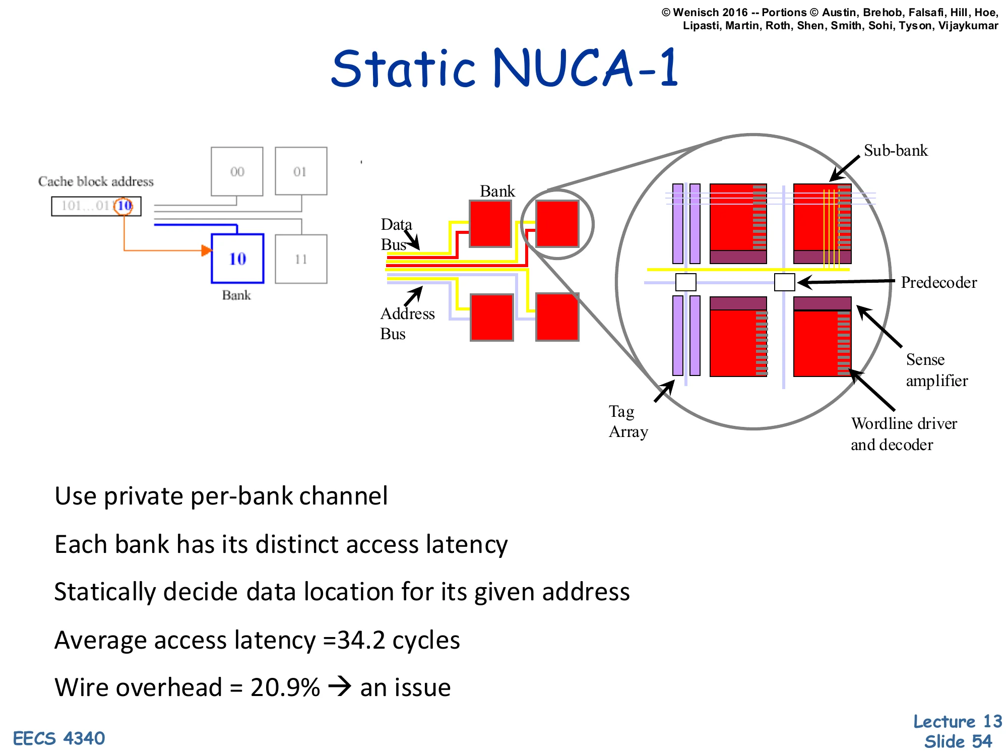
Show slide text
Static NUCA-1
[Diagram: A 4-bank array with each bank fed by its own private address+data bus from the CPU. The cache block address selects which bank using a few bits (“10” in the example). A magnified view shows a bank built of sub-banks with their own predecoder, sense amplifier, wordline driver, and tag array.]
- Use private per-bank channel
- Each bank has its distinct access latency
- Statically decide data location for its given address
- Average access latency = 34.2 cycles
- Wire overhead = 20.9% → an issue
S-NUCA-1 (Static NUCA, version 1) gives every bank its own private address and data bus to the CPU. Each bank is reached via its own dedicated channel, so different banks can be accessed in parallel without contention, and each bank’s latency is exactly its bank-access time plus its wire delay — no interference. Static means the address-to-bank mapping is fixed: a few bits of the address determine the bank. The cost is the wire overhead — 20.9% of the L2 area is just busses, because each bank needs its own pair of wires from the CPU. The average access latency of 34.2 cycles is far better than the worst-case 47 of the uniform cache, because most accesses hit nearer banks. The magnified view of a single bank shows the sub-bank structure (predecoder, sense amplifier, wordline driver, tag array) — this is just SRAM organization detail and is dense; the important content is the per-bank private bus diagram on the left half.
Static NUCA-2
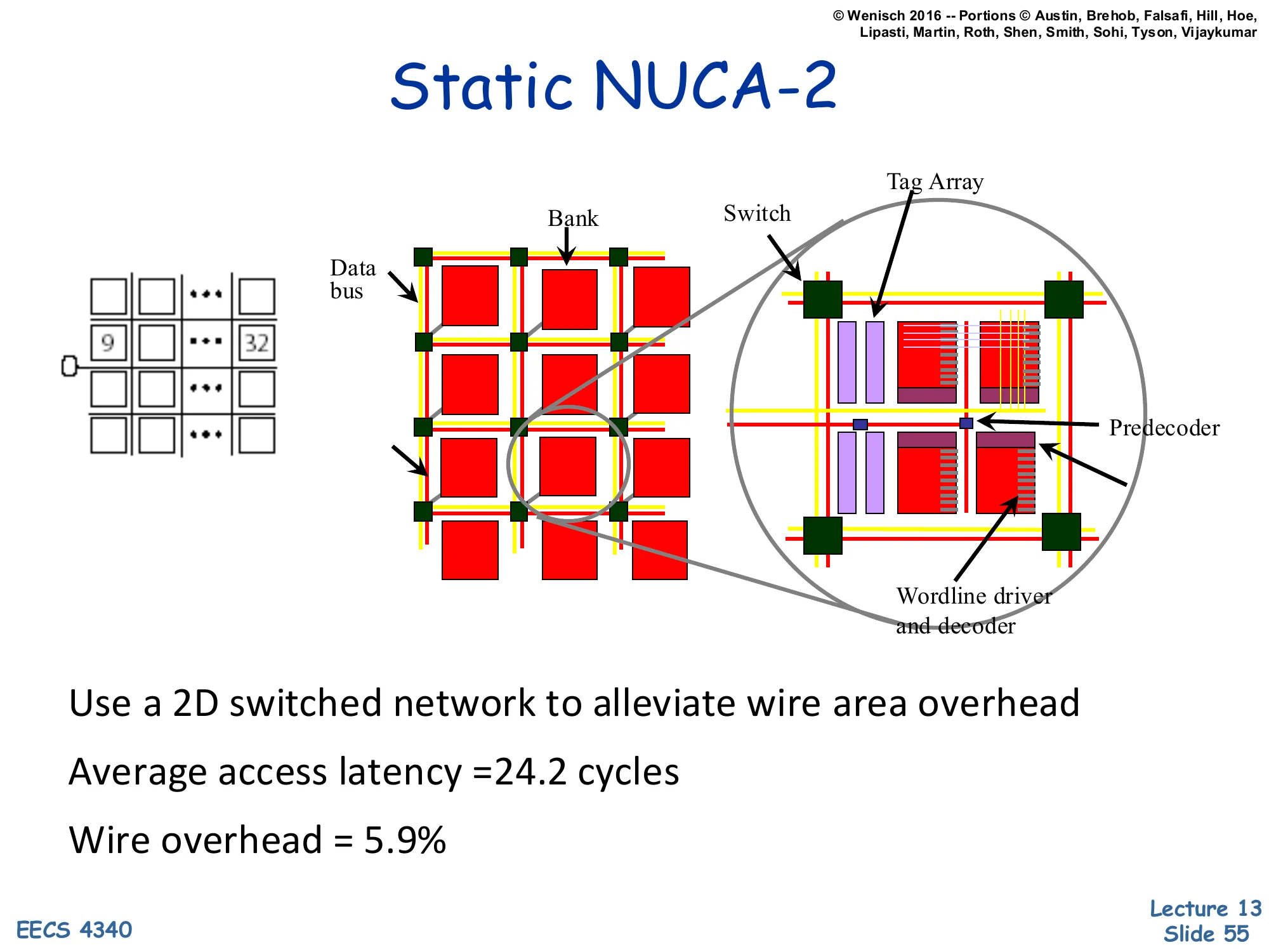
Show slide text
Static NUCA-2
[Diagram: A 2D grid of banks connected by switches — a switched mesh interconnect between banks instead of private busses. A magnified bank shows tag array, switch, predecoder, wordline driver and decoder.]
- Use a 2D switched network to alleviate wire area overhead
- Average access latency = 24.2 cycles
- Wire overhead = 5.9%
S-NUCA-2 replaces the per-bank private busses with a 2D switched network (essentially a small NoC). Banks are tiles in a mesh; messages between the CPU and a bank route through intermediate switches. This dramatically reduces wire area (5.9% vs 20.9%) because the wires are shared. Counterintuitively, the average access latency decreases to 24.2 cycles (from 34.2) — switched routing is more direct than the long parallel busses, despite the per-hop switch cost. Static still means address-to-bank mapping is fixed; the optimization is purely in the interconnect. This is the design that became influential — modern shared LLCs (e.g., Intel’s ring-bus L3, mesh-based server LLCs) all use some form of switched-network NUCA. The diagram is dense; the load-bearing content is the switched-mesh visual on the left and the latency/overhead numbers.
Dynamic NUCA (migration)
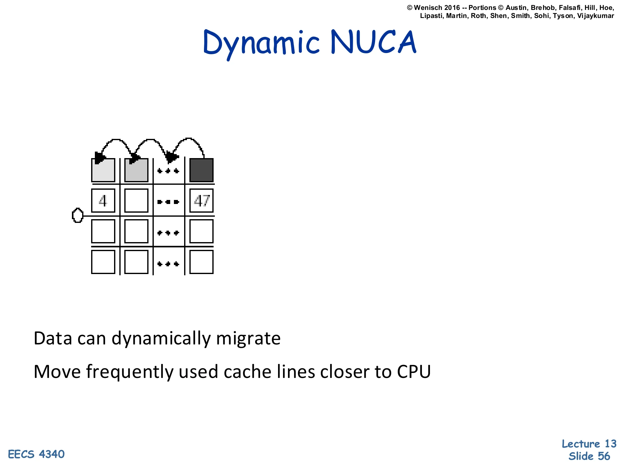
Show slide text
Dynamic NUCA
[Diagram: A 4×4 grid of banks. Hot data (line 47, top-right) migrates leftward through the top row toward the CPU at the left. Line 4 is already in a near bank.]
Data can dynamically migrate
Move frequently used cache lines closer to CPU
D-NUCA (Dynamic NUCA) extends S-NUCA-2 with data migration: a line that is accessed repeatedly migrates toward the CPU, hop by hop, so that hot data ends up in the nearest banks. The intuition is that working sets are typically much smaller than the cache, so the most-used lines should sit in the cheapest-latency banks. The arrows in the diagram show a line at “47” (a far bank) gradually moving leftward through the top row toward the CPU on the left. The challenge — solved by the various “mappings” on the next slides — is how to decide where a line lives at any given time, since the CPU now has to find the line as well as access it. Three mapping policies follow: simple, fair, and shared.
Dynamic NUCA — Simple Mapping
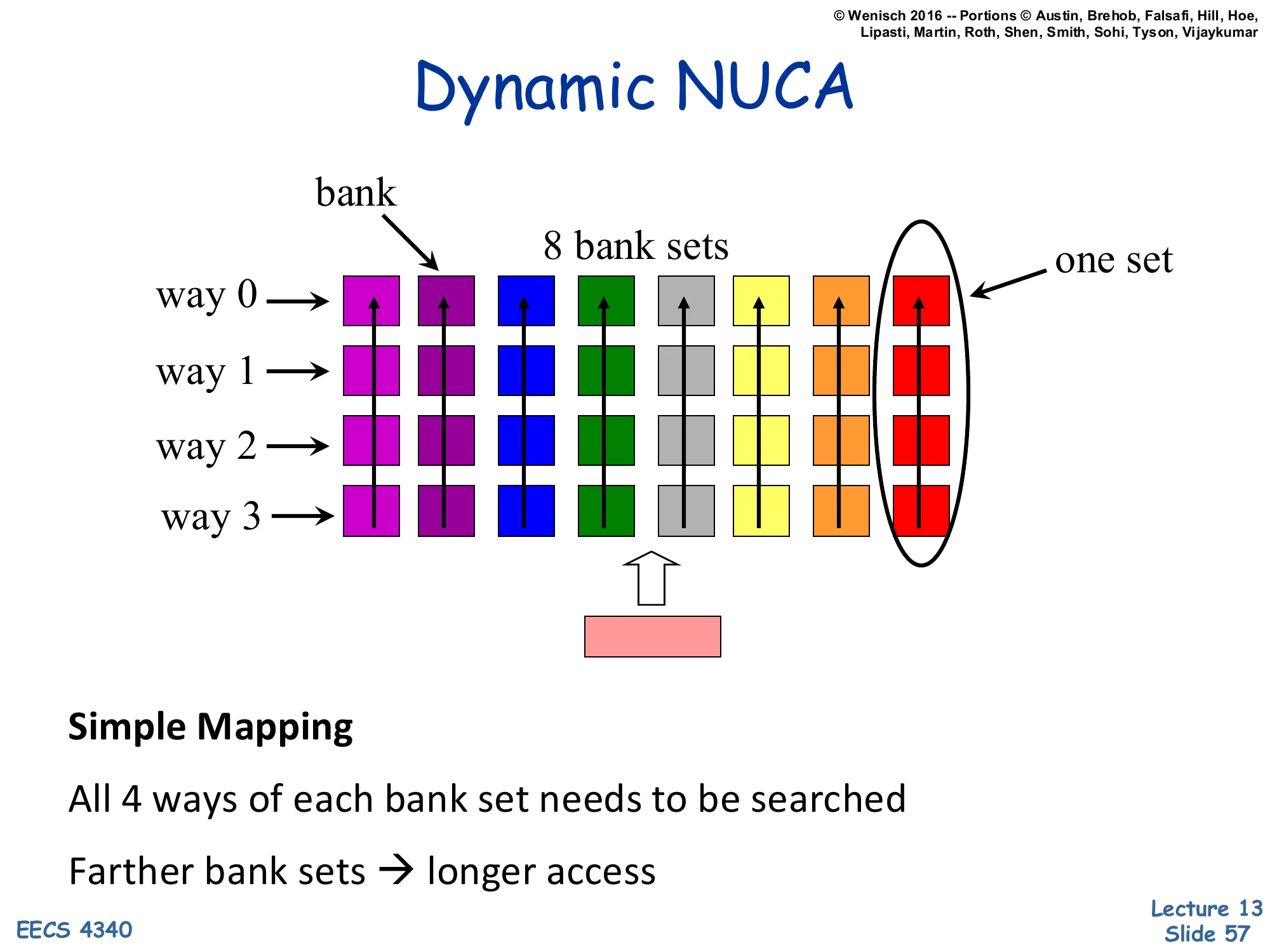
Show slide text
Dynamic NUCA
[Diagram: Eight bank-set columns, each containing four ways (way 0–3 stacked vertically). Different colors per column (8 bank sets). “One set” = a column of 4 ways. The CPU is at the bottom and probes upward through one bank set.]
Simple Mapping
All 4 ways of each bank set needs to be searched
Farther bank sets → longer access
Simple mapping: each address maps to one bank-set (by its index bits, like in a normal set-associative cache). The 4 ways within that bank-set sit on top of each other in the same column, so all 4 are at roughly the same distance from the CPU. To find a line, the CPU searches all 4 ways of the matching bank-set. The good news is that ways within a set have similar latency (so probe order doesn’t matter much). The bad news is that addresses mapped to farther bank-sets pay a longer access penalty for every one of their 4 ways — there is no way to escape the wire-delay tax of an unlucky set. This is the simplest D-NUCA scheme but also the one that benefits least from migration, since migration only happens within a set’s column. The diagram is colorful and reasonably legible; each column is one of 8 bank-sets, each containing 4 ways.
Dynamic NUCA — Fair Mapping
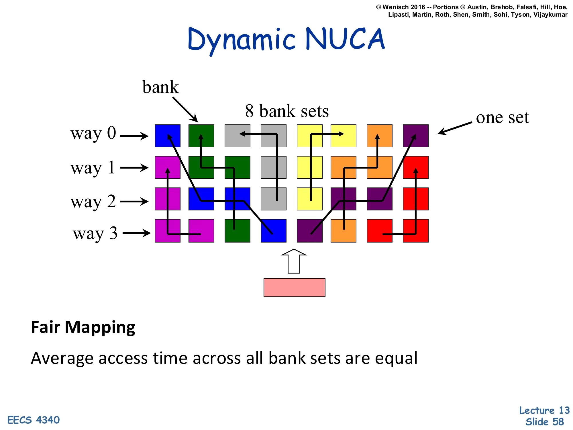
Show slide text
Dynamic NUCA
[Diagram: Eight bank-sets but with their 4 ways scattered across the bank grid — way 0 of one set might be at the top-left, way 1 across the grid, way 2 in the middle, way 3 at the right. Arrows trace the membership of each set across the chip.]
Fair Mapping
Average access time across all bank sets are equal
Fair mapping fixes the unfair-bank-set problem of simple mapping. Instead of stacking all 4 ways of a set in one column, the 4 ways are scattered across the grid so that every set has some ways near and some ways far. The result is that every set has the same average access latency — fairness across addresses. The cost is a more complex search: to find a line, the CPU must probe all 4 ways which are now in different banks. With migration, the most-used way of each set will gravitate to the nearest bank, so the actual hit latency for hot lines stays low. The diagram shows colored squares scattered with arrows tracing way-0/1/2/3 of each set across the grid — visually busy but the message is clear: ways are not stacked, they are spread.
Dynamic NUCA — Shared Mapping
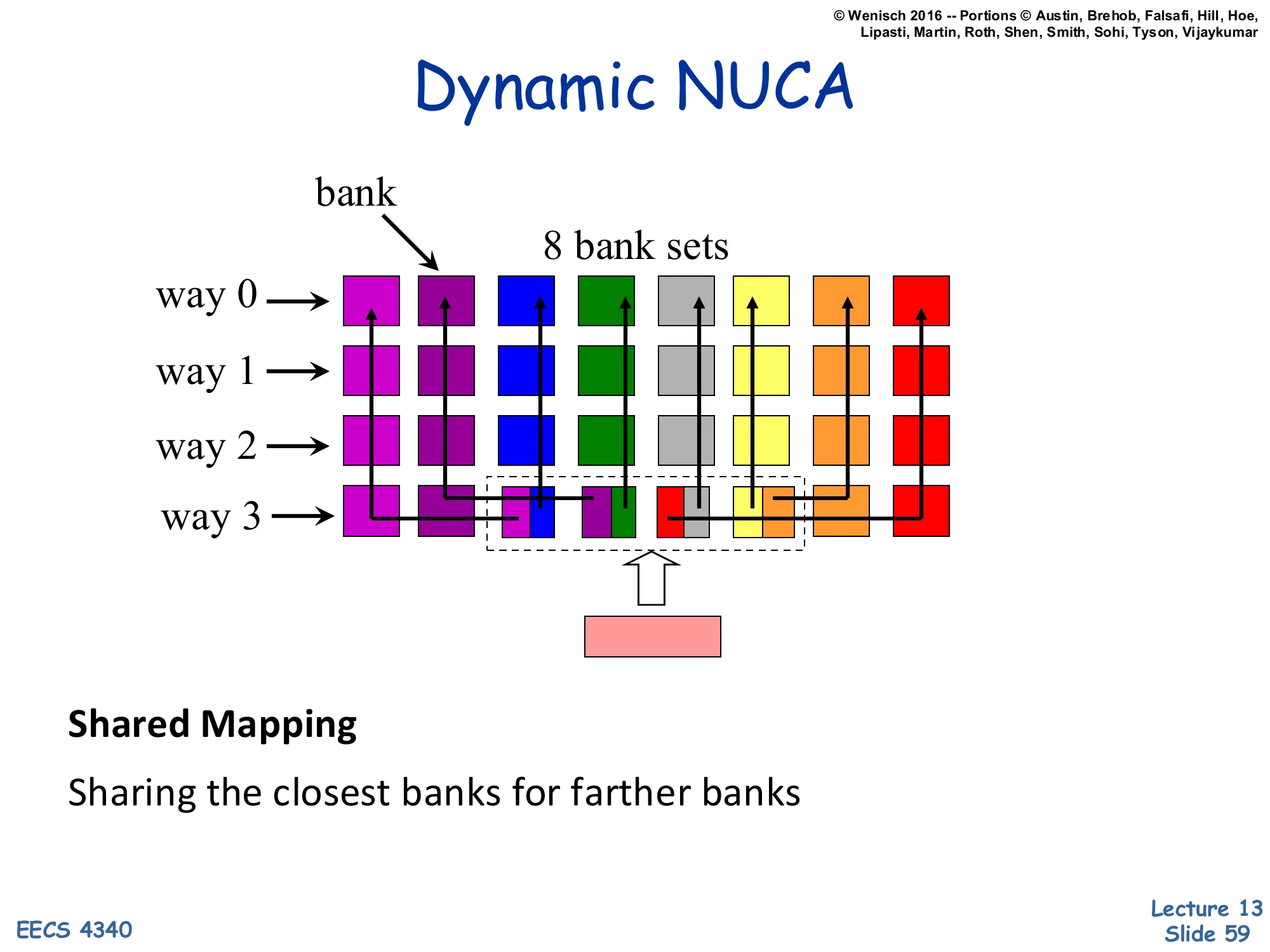
Show slide text
Dynamic NUCA
[Diagram: Like simple mapping (column-stacked sets) but with extra arrows showing far bank-sets sharing near banks for some of their ways — a dashed group highlights this shared region.]
Shared Mapping
Sharing the closest banks for farther banks
Shared mapping is a refinement: bank-sets retain their column structure (mostly simple), but the closest banks are shared across multiple far bank-sets. So a far bank-set has, say, 3 of its 4 ways in its own far column and 1 way in a shared near bank. The shared near bank serves as a fast home for the hottest member of each far bank-set, while the cold members stay in the far column. This is a compromise between simple (clear ownership, no near-bank for far sets) and fair (everyone gets near and far ways but search is complex). The complexity moves to figuring out which far bank-set currently owns the shared near slot — a kind of mini-coherence problem within the cache. The diagram shows the share group as a dashed region in the middle of the grid; the lines connecting far sets to their shared near banks indicate the sharing relationship.
Readings
Show slide text
Readings
For today:
- H & P Chapter 2.2, 2.3, and Appendix B.3
- Improving direct-mapped cache performance by the addition of a small fully-associative cache and prefetch buffers, https://dl.acm.org/doi/abs/10.1145/325096.325162
For next Monday
- A primer on hardware prefetching, https://link.springer.com/book/10.1007/978-3-031-01743-8
Announcements

Show slide text
Announcements
- Project #4
- Due: 22-April-26
- Final exam
- Friday, May 8, 2026, 9 AM – 12 PM, Mudd 633
- Project meetings
- Mondays and Wednesdays during my office hours